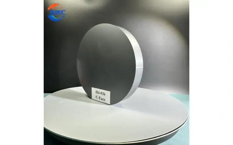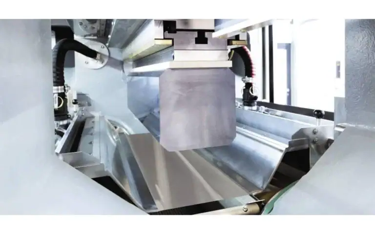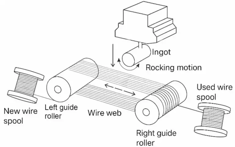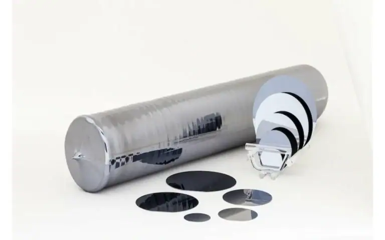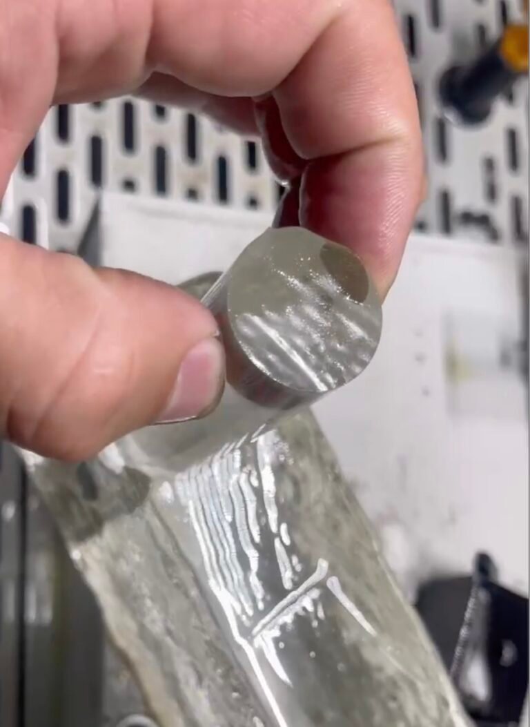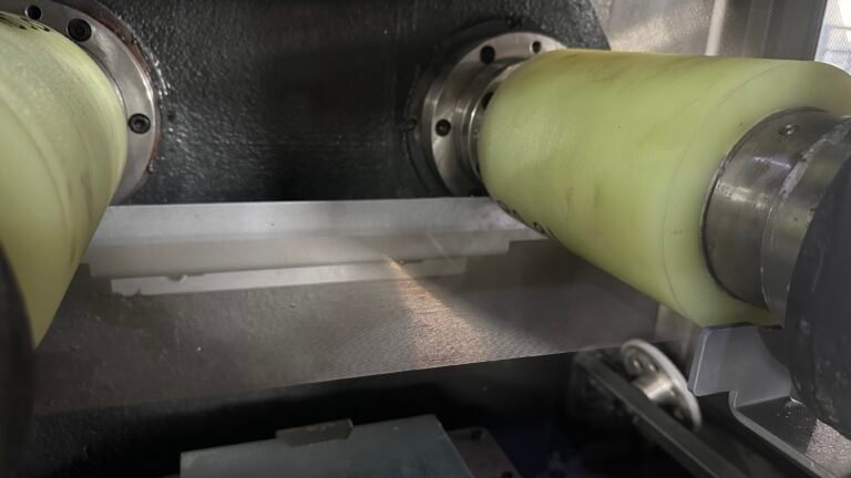
Choosing a semiconductor material cutting machine starts with identifying the manufacturing stage. Preparing a crystal blank, slicing an ingot into wafers and separating devices from a processed wafer are different jobs. The material name alone does not determine the equipment, and a machine used for one stage should not be assumed to perform the others.
This guide focuses on defining the cutting operation before selecting equipment for semiconductor and related substrate materials. It separates upstream material preparation from device singulation and explains what information to include in an application enquiry.
Which semiconductor material cutting stage do you need?
| Stage | Incoming workpiece | Required output | What to specify |
|---|---|---|---|
| Blank preparation | Crystal or material block | A blank with the required dimensions or cut faces | Cut location, orientation, geometry, workholding and allowance |
| Ingot slicing | A prepared ingot or blank | Individual wafers or parallel slices | As-cut thickness, slice arrangement, inspection criteria and batch size |
| Wafer finishing | As-cut wafers | Wafers meeting the required surface and dimensional specification | Stock removal, flatness, surface condition and handling requirements |
| Device singulation | A processed wafer containing devices | Separated dies | Device layout, separation streets, wafer support and the qualified singulation process |
Wafer slicing produces wafers from the starting material; dicing separates dies from a wafer later in the manufacturing route. These distinctions are illustrated in this semiconductor manufacturing process overview. The appropriate order and equipment for an actual line must be established from its process requirements.
Why is slicing different from wafer dicing?
For ingot slicing, the discussion begins with the blank and the wafers or sections to be produced. For dicing, the incoming wafer already has a device layout that constrains where separation can occur. The fixtures, alignment requirements and acceptance criteria therefore need to be specified for the relevant operation.
A diamond wire saw is not a laser system. Descriptions of laser dicing do not establish a capability of the wire-saw models listed on this site. Likewise, a model described for substrate slicing should not be offered as a device-dicing machine without a separately verified application and configuration.
How should the material be described?
Provide the material identity and grade, crystal orientation where applicable, incoming dimensions and any known variation in the blanks. Explain whether the cut is intended to produce a test specimen, a substrate or a production batch. Identify existing coatings, bonded layers or other features that affect how the workpiece can be held and handled.
Keep the application categories precise. Silicon and silicon carbide may be semiconductor workpieces, while sapphire and technical ceramics can have substrate or other supporting roles. Grouping them as hard and brittle materials does not establish that they share a cutting recipe or inspection standard.
For sapphire intended for LED substrate preparation, refer to the sapphire slicing application guide. Detailed material-specific pages remain separate from this process-stage overview.
Which equipment pages are useful starting points?
Use the following links to review a proposed configuration with the technical team. They are product entry points, not proof that any listed machine can meet an unspecified drawing.
- Individual cutting tasks: review the SVO-40 single-wire page and confirm the required cut path, fixture and operating envelope.
- Parallel batch slicing: begin with the multi-wire model overview and compare the blank arrangement with the intended output.
- Thin-wafer slicing discussions: consult the SOMI2-600S product page, then confirm the material and complete acceptance specification.
- Oscillating multi-wire configurations: review the SOMIS-400 product page when discussing the appropriate arrangement for the proposed material.
No common minimum thickness, cutting accuracy or throughput is assigned to these models here. Model-specific limits and options must come from the corresponding technical documentation and the agreed trial.
What happens after a wafer has been sliced?
An as-cut wafer should not automatically be treated as a finished substrate. Subsequent operations depend on the required surface and geometry. For example, this silicon wafer production description distinguishes slicing from later lapping or grinding and polishing.
Define the finishing allowance before the cutting trial. Record which conditions are accepted directly after cutting and which will be established by downstream processing. Avoid a general promise that every cut surface needs no cleaning, grinding or polishing.
What should a trial and equipment enquiry include?
- Identify the incoming material and the manufacturing stage.
- Provide the drawing, blank dimensions and intended cut direction.
- State the as-cut requirements separately from finished-part requirements.
- Describe expected batch sizes, changeovers and handling constraints.
- Agree on a representative trial, inspection method and acceptance criteria.
- Review the quoted machine configuration, utilities, fixtures and support scope.
Use the precision slicing quality-check guide to define inspection inputs. For configuration and quotation comparisons, see the diamond wire slicing process and cost guide.
Send these details through the equipment enquiry page. A clearly identified manufacturing stage gives the team a practical basis for recommending which configuration should be evaluated and what the trial needs to demonstrate.