
Wafering turns a crystal ingot into wafer blanks and then prepares those blanks for their receiving process. For a typical polished silicon substrate, the route runs through crystal growth, cropping and shaping, slicing, mechanical flattening, etching, polishing, cleaning and inspection.
The wafering process is a sequence of operations with different jobs. Growth establishes the starting crystal. Cutting establishes the blank geometry. Later removal and surface preparation establish the condition the wafer must have before it enters its next application. A successful cut is one step in that sequence.
This guide follows that route in order, using silicon wafer manufacturing as the main example. Other crystals need their own qualified growth, etching and finishing processes. Vimfun SOM200 is introduced at the slicing stage, where its documented silicon application is relevant; it is not presented as equipment for every stage of wafer production.
What Does the Wafering Process Include?
The simplest way to understand the route is to follow what happens to the material. It begins as a grown ingot, becomes a prepared section, separates into blanks, and then receives the dimensional and surface treatment required by the substrate drawing.
| Stage | What the operation does | Material leaving the stage |
|---|---|---|
| Crystal growth | Produces the required starting crystal | Identified ingot |
| Cropping and shaping | Selects usable sections and prepares their outside geometry | Stock ready for mounting |
| Slicing | Separates stock into wafer blanks | As-cut slices |
| Grinding or lapping | Establishes the required intermediate geometry | Mechanically flattened blanks |
| Etching | Removes material chemically under the qualified substrate route | Etched blanks ready for subsequent finishing |
| Polishing | Establishes the specified finished surface condition | Polished wafers |
| Cleaning and inspection | Removes process residues and checks the receiving requirements | Accepted, identified substrates |
These are process functions, not a requirement to buy one separate machine for every row. Some routes combine operations or use a different order for an intermediate treatment. The table explains the conventional sequence; the actual wafering specification must say which operations and receiving states apply. The BYU wafer fabrication overview provides background on silicon crystal growth and substrate preparation.
Step 1: Grow the Starting Crystal
Wafer production starts upstream of the saw. Crystal growth produces the ingot from which the substrates will be made. In the Czochralski route for silicon, a seed is used to grow a crystal from a melt as the pulling and rotation conditions are controlled. Float-zone growth is another route used for appropriate silicon requirements.
In wafering, growth and slicing solve different problems. The growth route and material specification establish characteristics such as crystal identity and the intended electrical properties. Wafering cannot turn an unsuitable ingot into the required grade simply by cutting it accurately.
In silicon growth, intentional doping is part of establishing the specified electrical properties. The saw then receives that identified material; it does not set the dopant concentration.
Before the ingot leaves growth, retain its identification and the available orientation information. The machining team needs to know which section is supplied and how the intended wafer plane is identified. A cylindrical shape alone does not establish those properties.
For the equipment and process at this upstream stage, see the crystal growing furnace page. The cutting enquiry should reference the material that the growth operation actually supplies, rather than asking the saw quotation to establish a crystal specification that has not been agreed.
Step 2: Crop and Shape the Ingot
The grown ingot must be prepared before a repeated slicing layout can be established. Cropping divides it into useful sections and removes material excluded by the approved plan. Shaping prepares the outside geometry needed for the specified substrates and the mounting arrangement.
For round substrates, the preparation route concerns the required cylindrical geometry and locating references. A different retained cross-section belongs to a different product drawing. Do not add a squaring operation merely because the equipment can make one.
This part of wafering also establishes the usable material boundary. The full incoming length, the retained section and the end allowances are different quantities. Draw the portion that will enter the slicing operation before estimating how many blanks it can supply.
Keep the crystal reference through preparation. If a face or mark will be removed, transfer the locating information by the approved procedure before machining changes it. A convenient prepared surface is a mechanical datum; its relationship to the required crystal plane still needs to be established.
The output of this wafering stage is prepared stock, ready for mounting. It should fit the mounting plan, retain the required references and leave enough usable material for the intended slicing layout.
Step 3: Slice the Stock into Wafer Blanks
Slicing is the wafering stage where the ingot becomes separate blanks. A diamond-wire arrangement uses an abrasive cutting path through the mounted stock. In a multi-wire configuration, parallel wire paths separate several blanks within the same setup. The multi wire saw overview explains the equipment configurations used for that duty.
The wafering layout must distinguish the blank thickness from the material removed in each cut. It must also reserve the material that later grinding, lapping, etching or polishing will remove. Setting the saw to the final wafer thickness can leave the receiver without enough stock to complete its work.
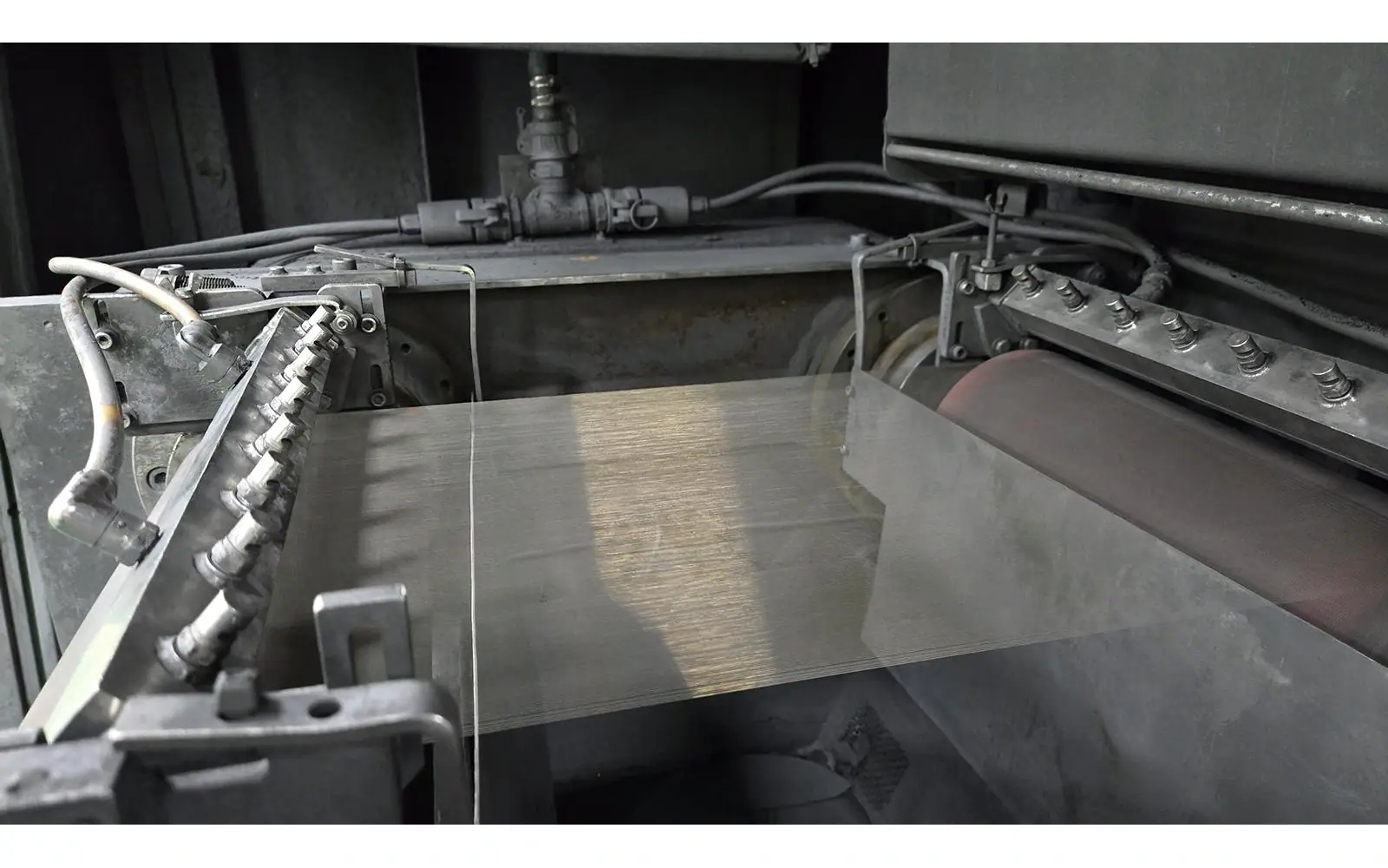
Workholding supports the stock through entry, the main cut and final separation. Where a bonding arrangement is used, the mounting and release procedure are part of the approved process. They determine how the separated pieces can be taken off the fixture without losing their identity or required references.
Line speed, tension and feed must be assessed together for the actual material, wire and geometry. No material-specific operating recipe is established here. For wafering trials, request the conditions used during cutting and the measured blank result, rather than treating an equipment maximum as a suitable production setting.
After the cut, release and identify the slices. Retain their order when the investigation needs to relate a thickness trend or defect to a position in the original stock. These pieces are now wafer blanks; the next stages establish the required geometry and surface condition.
Step 4: Flatten the Blanks by Grinding or Lapping
The as-cut blank proceeds to mechanical preparation when the substrate route requires it. Grinding and lapping remove stock to flatten the faces and reduce the saw-marked surface. Grinding uses a fixed abrasive tool; lapping uses an abrasive working interface against a lap. They should be specified by the condition required after the operation, rather than described as interchangeable ways to make a slice look smooth.
For wafering, separate the nominal thickness target from thickness variation and shape requirements. A blank can be uniformly too thin, or meet an average thickness while a local region has insufficient remaining stock. The receiver needs a defined measurement area and process state to interpret the result.
The grinding and lapping equipment page covers the mechanical-finishing equipment context. Selection should follow the actual blank dimensions, material and receiving specification. A saw capability or a photograph of a flat plate does not establish this stage’s performance.
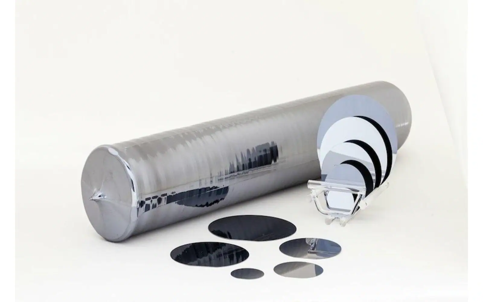
Mechanical removal changes the thickness available for subsequent treatment. Keep the as-cut and post-flattening values separately so the wafer manufacturing route can account for where stock is consumed. If a later operation requires more removal, revisit the blank allowance instead of assuming that polishing will correct every earlier dimensional problem.
Step 5: Etch under the Qualified Substrate Process
Etching removes material chemically. In the substrate-preparation sequence, it has a different role from mechanical flattening and from polishing. In conventional silicon preparation, chemical removal can address the surface layer affected by earlier machining before subsequent polishing. The wafering route specifies the treatment and removal needed for that material.
Here, etching means a substrate-preparation operation. It is not a discussion of patterned device etching used to create circuit features. Keeping those two meanings separate prevents the wafer manufacturing guide from drifting into semiconductor device fabrication.
The chemistry and removal conditions depend on the material and approved route. A silicon treatment must not be assumed suitable for SiC, sapphire or another crystal. This overview therefore describes the operation’s purpose without supplying an unqualified chemical recipe.
Etching also belongs in the material allowance. Record the thickness state before and after the applicable treatment, and identify how the wafer is cleaned before the receiving operation. For wafering decisions, an etched surface and a polished surface must not be reported as the same delivered condition.
The question for the next station is concrete: does the treated blank have the stock, geometry and surface condition required for polishing? Resolve that question under the receiver’s inspection method, rather than relying on the appearance of one selected sample.
Step 6: Polish to the Specified Surface Condition
Polishing reduces the remaining surface roughness and establishes the finished surface required by the substrate route. The drawing may require treatment of one face or both, with its own geometry and inspection conditions. A mirror-like appearance is a visible observation; it is not a complete wafer acceptance specification.
At this stage of wafering, the remaining removal allowance must still support the final requirement. If the earlier blank target left insufficient stock, extra polishing cannot create the missing material. This is why the slicing target should be chosen from the complete removal route rather than from the final nominal thickness alone.
Keep polishing separate from earlier flattening in the process description. They may contribute to the same final part, but their output states and inspection questions differ. The useful wafer production report identifies the condition after each relevant operation instead of assigning every improvement to the saw.
Determine the actual receiver’s requirements before treating the wafer as finished. Thickness, surface condition and other specified features must be assessed by the applicable methods. Neither a photograph nor an equipment label proves that all of those checks have passed.
For wafering, the practical output is a substrate prepared to a stated condition. It is ready for the next agreed application when that receiver accepts it, rather than simply when the last polishing step ends.
Step 7: Clean, Inspect and Package the Wafers
Cleaning removes the residues associated with the applicable processing route. Inspection then checks the conditions specified for receipt. Packaging and identification preserve that accepted state during transfer. These operations complete the wafering route described here; circuit fabrication is a later and different subject.
Record what was actually inspected. Nominal thickness, thickness variation, bow or warp and surface observations are separate features. A central thickness reading cannot establish a thickness map, and visible edge condition cannot establish every internal defect requirement.
The Stanford wafer specifications illustrate that wafer descriptions distinguish material, orientation, thickness and surface treatment. They are reference specifications, not acceptance evidence for a Vimfun trial or an instruction to copy a particular value into another customer’s drawing.
Retain lot identity and the inspected state with the accepted pieces through packaging and transfer.
Where Vimfun Equipment Fits in the Route
The Vimfun SOM200 small multi wire saw is a slicing-stage reference. Its product introduction lists silicon among the application materials, a maximum workpiece envelope of 200 × 200 × 200 mm and a configurable slice range of 0.3–12 mm. These are machine-configuration entries, not guaranteed finished-wafer results for every material and setup.
Use those entries to start an equipment discussion about the proposed stock. For wafering, the supplier still needs the actual geometry, plane, blank target and receiving condition. Larger batch layouts or different stock dimensions should be reviewed through the wafer slicing machine selection rather than forced into a small-format example.
Ask which operations the proposal includes. A multi wire saw separates the blanks; it does not become the crystal grower, etching process and polishing system by being described as part of a production line. Link the equipment scope to the stage it performs and qualify that stage’s output against the next operation.
Which Page Answers the Next Question?
This article explains the complete wafering process. Use the narrower equipment and application pages when the next question concerns one stage.
| Your question | Read next | Scope |
|---|---|---|
| How is the starting ingot produced? | crystal growing furnace | Growth and its equipment |
| Which setup should separate the blanks? | wafer slicing machine | Slicing equipment selection |
| How are repeated cutting paths arranged? | multi wire saw | Multi-wire configuration |
| Which operation prepares the mechanical geometry? | grinding and lapping equipment | Mechanical finishing |
FAQ
Is wafering the same as making integrated circuits?
No. Wafering prepares substrates from bulk crystal. Circuit fabrication uses suitable wafers in subsequent device-processing operations. This guide ends at the specified substrate condition rather than following lithography, patterned etching and other device steps.
Does every material use the same sequence?
The sequence explains a conventional polished-silicon route. Other materials and receiving requirements can change the qualified operations. Wafering process selection must identify which treatment and final state apply; it should not transfer a silicon etching or polishing procedure to another crystal by default.
Is the as-cut target the finished wafer thickness?
Not when later removal is required. The wafering blank needs sufficient stock for the approved grinding or lapping, etching and polishing route. Specify the as-cut and finished states separately, then measure the relevant condition at each stage.
For a useful trial request, send the identified stock, intended plane and blank drawing, and tell the supplier which operation receives the slices. That lets the cutting proposal support the complete route while remaining accountable for the operation it actually performs.