Silicon Wafer Sizes and Thickness: A Reference Table
Silicon wafer thickness depends on diameter, wafer type and process stage. Use sourced reference ranges and specify the actual blank requirement.
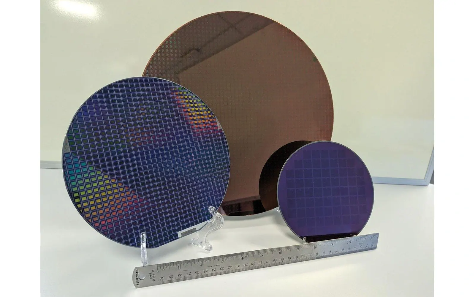
Silicon wafer thickness in a reference table is not the saw's blank target. A polished-substrate specification and an as-cut requirement describe different process stages. Put finishing stock, local thickness limits and the measurement method on the drawing before choosing slice spacing.
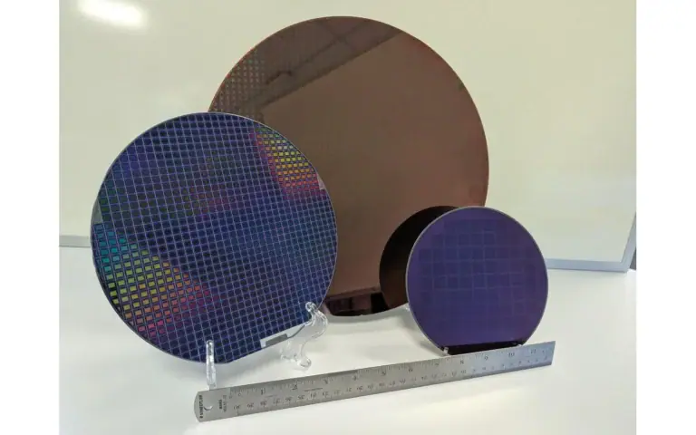
Diameter is useful for sizing equipment, but it does not uniquely determine silicon wafer thickness. The sourced ranges below are examples from identified documents, not a replacement for the customer's current wafer specification.
Vimfun SOM200 lists a configurable slice range, but a catalogue range is not a recommendation for silicon wafer thickness. Define the required blank state and later removal before using a machine reference in the enquiry.
Read Silicon Wafer Thickness in Context
A specification may describe thickness at a particular location, an average or limits across the evaluated area. It may also define total thickness variation separately. Those details are necessary to interpret the requirement; a nominal value alone leaves too much ambiguity.
The SEMI M1 scope summary concerns specified polished single-crystal wafers and distinguishes them from other wafer categories. It is a standards reference, not evidence that a particular as-cut blank satisfies the full standard.
A Sourced Reference Table
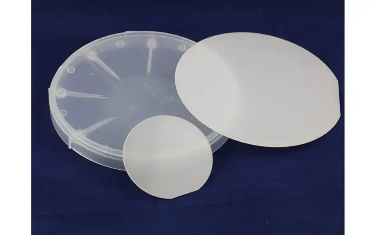
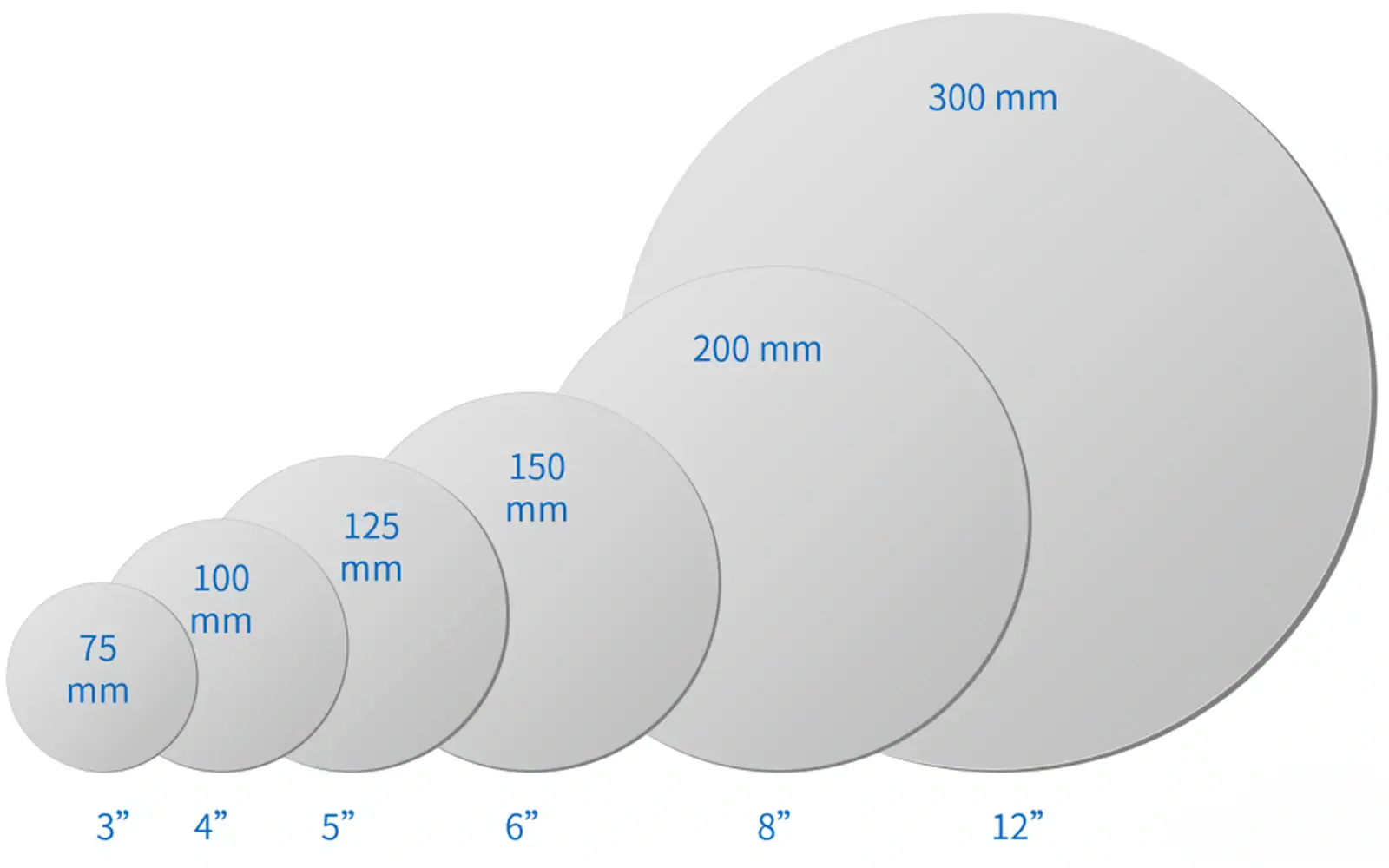
Silicon wafer sizes identify diameter categories, while standard silicon wafer thickness depends on the substrate specification and process stage. Read the table as a set of sourced reference examples, not a universal purchase standard. A custom research wafer or a later-thinned substrate can depart from these examples without contradicting its drawing.
The following values reproduce dimensional ranges in City University of Hong Kong teaching material and an example in Stanford's wafer specification sheet. They are reference examples from those documents, not a claim about today's universally required dimensions. The customer's applicable specification and revision remain controlling.
| Diameter | Thickness reference | Source and interpretation |
|---|---|---|
| 100 mm | 475–575 µm for listed single-side-polished examples | Stanford specification sheet; particular wafer categories |
| 125 mm | 0.60–0.65 mm | City University teaching table; typical specification example |
| 150 mm | 0.65–0.70 mm | City University teaching table; typical specification example |
| 200 mm | 0.715–0.735 mm | City University teaching table; typical specification example |
| 300 mm | 0.755–0.775 mm | City University teaching table; typical specification example |
Sources: City University wafer preparation notes and Stanford wafer specifications.
Do not merge the ranges into a new standard or attach machine tolerances to them. These examples show why silicon wafer thickness must be associated with a defined wafer category. They do not establish limits for solar wafers, custom research substrates or a downstream thinning operation.
Are the units and tolerance actually stated?
Millimetres and micrometres often appear in the same project. State the unit in every drawing and table heading. Converting 0.725 mm to 725 µm changes the notation, not the physical thickness. An omitted unit can create a much larger error than an ordinary process variation.
When reviewing silicon wafer thickness, distinguish a decimal value from a tolerance. A target of 0.725 mm does not imply that every measured location must be exactly that thickness. The tolerance and measurement method must be written separately.
Commercial inch descriptions can also be approximate size names. Use the specified metric diameter when checking fixtures and receiving equipment rather than calculating a new acceptance diameter from the informal label.
The teaching-table 200 mm range, 0.715–0.735 mm, converts to 715–735 µm. Its 300 mm range, 0.755–0.775 mm, converts to 755–775 µm. These conversions do not add precision, update the document or make its examples binding on a new order.
For silicon wafer thickness, keep the source category beside the number. The Stanford 100 mm examples and the City University teaching table serve different purposes. Do not combine them into a new “standard tolerance” assembled from unrelated rows.
I'd copy the approved target and tolerance directly into the blank drawing, with the unit in the field label. The pitfall is copying a familiar silicon wafer thickness value and then allowing the operator to infer the finishing allowance. That allowance should be approved by the receiving process, not guessed at the machine.
A reference value is not a purchase specification.
Does diameter determine the thickness?
A larger wafer may need a different handling and process arrangement, but diameter alone cannot settle its thickness requirement. Research wafers, test wafers, custom substrates and later-thinned wafers can differ from commonly encountered incoming substrates.
For silicon wafer thickness procurement, identify the wafer type and the operation at which the requirement applies. If a customer uses an unusually thin substrate, confirm whether it arrives thin, is supported on a carrier or is thinned after device processing. Those are different manufacturing routes.
Do not infer the capability of a slicing machine from a reference table of finished substrates. The machine's actual workpiece, blank thickness and quality requirements must be evaluated directly.
How much stock will finishing remove?
The saw produces a blank for a defined receiving process. Any stock removed by mechanical or chemical finishing must be included in the planned allowance. That allowance should come from the approved route, not an arbitrary percentage added to a reference thickness.
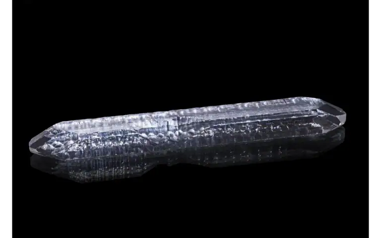
Use silicon ingot slicing as the application context, then document the actual handoff condition. A request for “standard wafers” is less useful than a drawing describing the required blank and its intended next step.
Silicon wafer thickness at the saw should be recorded independently of final thickness. Keep before-and-after measurements connected to the same sample if a finishing trial is used to establish the route.
Account for Cutting Width and Material Recovery
The repeating slice interval includes retained blank material and the effective cut. Increasing blank thickness changes the number of slices available from a usable section, while the cut and end allowances also consume material. A thickness choice therefore affects yield as well as handling.
Compare accepted recovery under the same finishing requirement. A thinner blank is not beneficial if it fails to provide enough stock or breaks during release. Likewise, a thicker blank may add finishing work that outweighs an apparent improvement in survival.
A silicon wafer thickness trial should record usable input, slice count, rejected material and the receiving operation's result. Keep geometric estimates separate from demonstrated output.
Measure More than One Point When Required
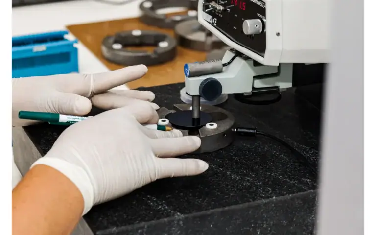
A single centre reading cannot establish thickness uniformity over the whole wafer. Select the measurement pattern and edge exclusion according to the acceptance requirement. Record the support condition, instrument method and whether the surface condition is suitable for measurement.
Total thickness variation describes the range over a defined area; bow and warp describe shape under defined conventions. A silicon wafer thickness target does not replace those criteria when they matter to the next operation.
For thin blanks, agree on handling and measurement before the trial. If the sample cannot be evaluated reliably with the available instrument, describe the limitation rather than presenting uncertain readings as proof of capability.
Check the Equipment against the Real Assembly
A machine assessment should include the mounted stock, fixture, desired slice spacing and release arrangement. The bare ingot diameter is only one input. Also confirm whether the production objective is an individual sample, a pilot batch or repeated multi-line output.
Review a wafer slicing machine against that actual requirement. The reference table above does not promise that one configuration covers every silicon wafer thickness or diameter listed.
Provide the receiving process and inspection criteria with the enquiry. That allows the supplier to propose a representative test instead of answering a broad dimensional question with a nominal machine envelope.
Write Separate Thickness Requirements for Each State
Give the final requirement and the intermediate requirement different names. A purchase order that repeats one thickness value across every process can leave the operator uncertain about whether it refers to an as-cut blank or a finished substrate. Put the state beside the number wherever it appears.
Silicon wafer thickness should be tied to an acceptance window, not only a nominal value. Ask which area is evaluated, what local departures matter and when the measurement occurs. The receiving team may need to preserve stock for its own processing, so a centre reading alone may not answer its question.
Do not use diameter as a shortcut for the thickness drawing. If a standard is part of the requirement, identify the applicable specification and agreed version. If the part is custom, identify it as custom and provide its own receiving condition. A familiar wafer size does not make every unstated requirement standard.
Keep allowances separate from cut losses. Material reserved for later removal remains in the blank; material removed by the saw does not. Combining the two in one allowance obscures the layout and can produce an incorrect slice-count estimate. Draw the repeated interval before using it in material planning.
When silicon wafer thickness changes, review handling and the fixture rather than adjusting only the guide layout. Ask how pieces will be supported through separation, how order is retained and whether the inspection arrangement still represents the requirement. This is a review of the proposed task, not a claim that every thinner blank necessarily fails.
The returned record should include as-cut observations and any later correction. If a supplier measures only after finishing, state that clearly. A corrected result cannot establish the original cutting condition unless the removed material and previous state are also documented.
Use the trial to settle an actual drawing question. It may concern the blank window, the finishing reserve or a measurement disagreement. Name that question before the run. A demonstration of the thinnest separable piece can be interesting, but it does not establish the thickness that the production receiver can accept.
| Decision field | Evidence to retain |
|---|---|
| Finished requirement | Nominal value, local window and receiver |
| Blank requirement | As-cut target and removal allowance |
| Measurement record | Area, process state and correction history |
Choose the Page That Answers Your Question
This article answers: Which thickness value belongs in the saw order? It does not replace the following equipment or application scopes.
| Your question | Relevant page | Boundary |
|---|---|---|
| Need the silicon ingot slicing context? | silicon ingot slicing | Application or process context for the receiving task |
| Need the wafer slicing machine context? | wafer slicing machine | Application or process context for the receiving task |
FAQ
Is final silicon wafer thickness the saw target?
Not when later operations remove stock. Silicon wafer thickness at final receipt and the as-cut target must be specified separately. The finishing team should approve the reserved material rather than leaving the saw operator to infer it.
Does diameter complete the silicon wafer thickness requirement?
No single diameter label completes the requirement. State the applicable standard or custom drawing and the receiving condition. Nominal size information is useful, but it does not replace the thickness window and inspection method.
What changes when the silicon wafer thickness target decreases?
Review finishing stock, support, release and measurement alongside the target thickness. Record what the trial actually establishes. A thin intact sample does not by itself demonstrate acceptable routine output for the complete route.
Write an Unambiguous Requirement
A practical specification identifies material, wafer category, diameter, required plane, as-cut thickness target, tolerance, evaluation area and finishing allowance. Add the accepted edge and surface condition and identify the measurement method.
Silicon wafer thickness is most useful as part of that complete requirement. Reference ranges can help a team ask better questions, but the approved drawing determines the actual work. Keeping the process stage and measurement definition visible prevents an ordinary reference value from becoming an unsupported production promise.
Use the reference table to identify questions, then issue the actual blank drawing. State silicon wafer thickness at the required process stage, its tolerance, inspection area and finishing allowance. Confirm the mounted envelope separately. Keep the reference document and current purchase specification distinct when comparing supplier proposals.