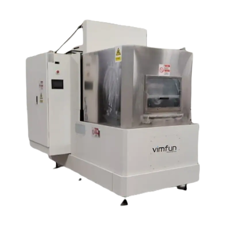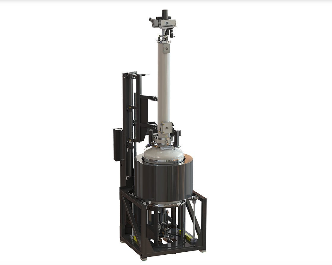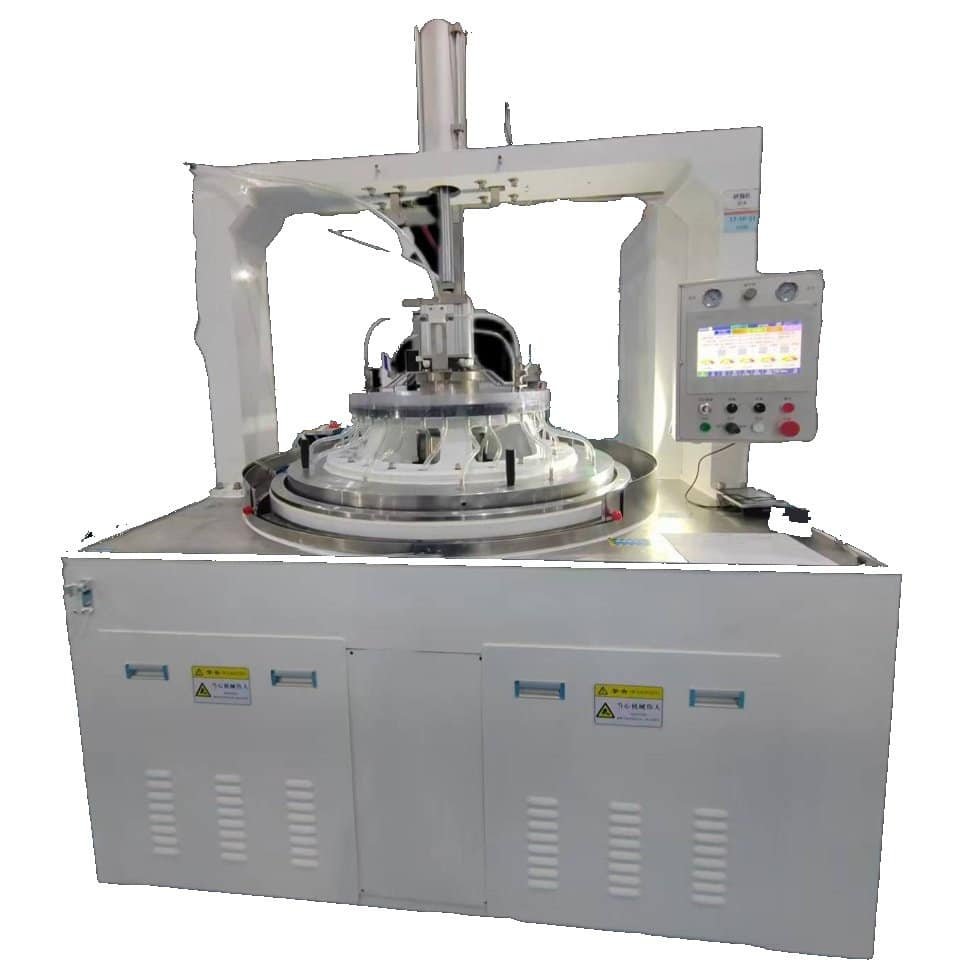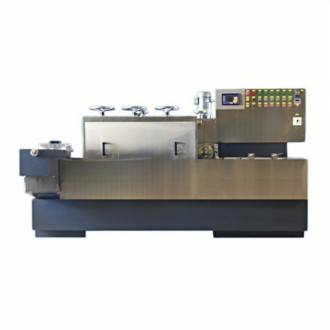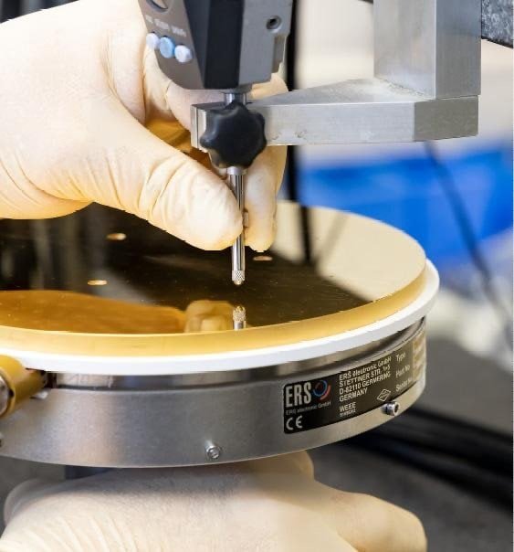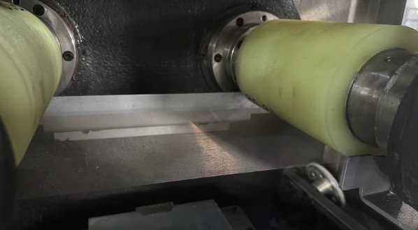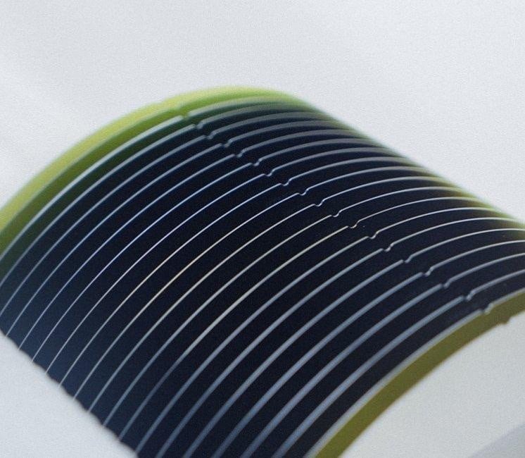
Complete Semiconductor Wafer Processing Equipment — Crystal Growth · Cutting · Lapping · Polishing
From ingot growth to polished wafer — Vimfun delivers the full equipment chain for Si, SiC, sapphire, and Ge semiconductor manufacturing.
N . A . Office
캐나다 위니펙, 매니토바주
전화 문의
(1)408-571-8651
오전 7:30 - 오후 7:30
7일
당사가 하는 일
Complete Equipment Solutions for Semiconductor Wafer Manufacturing
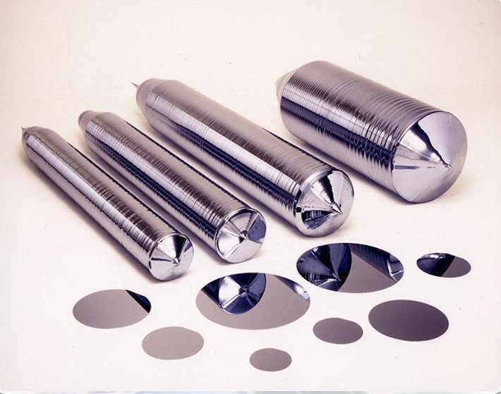
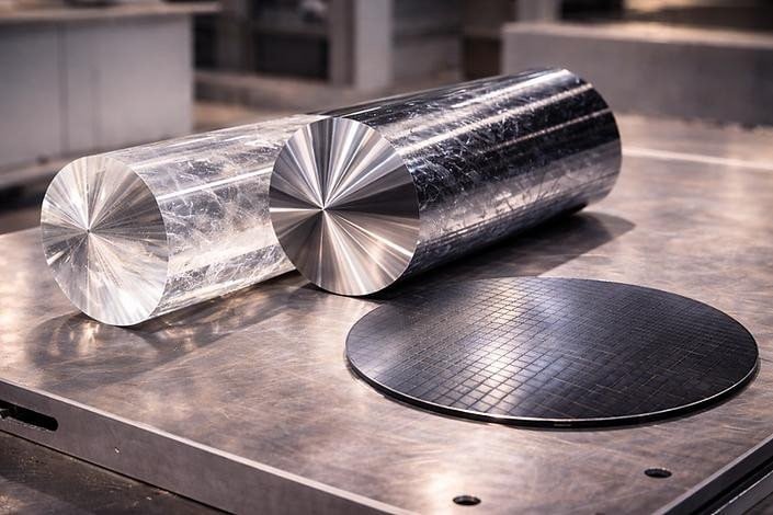
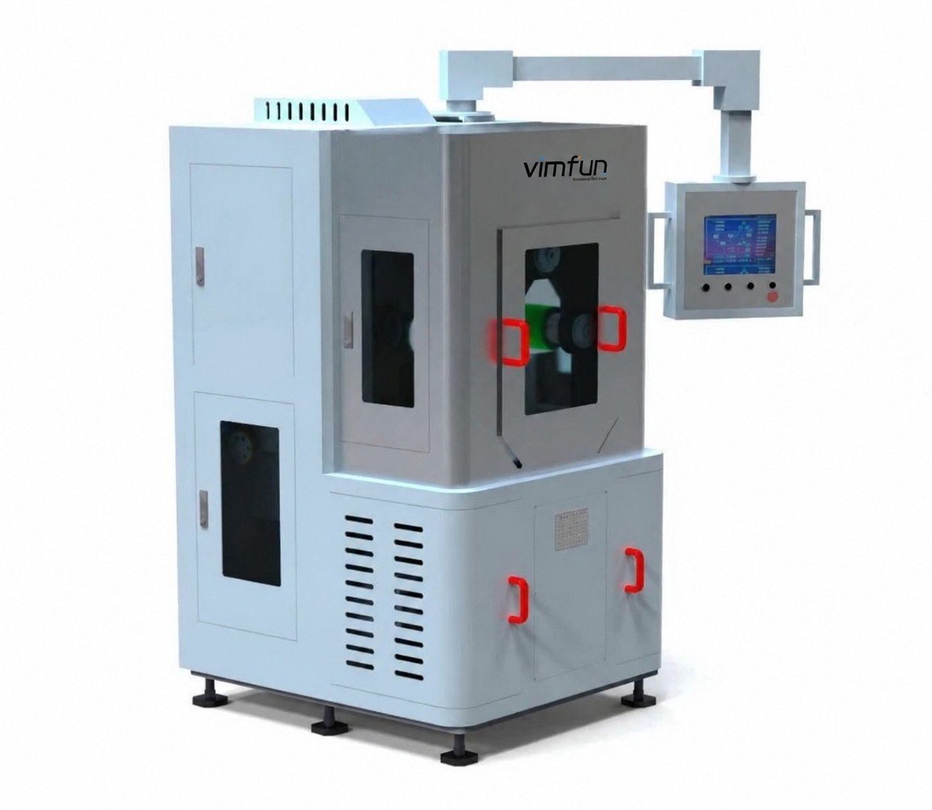
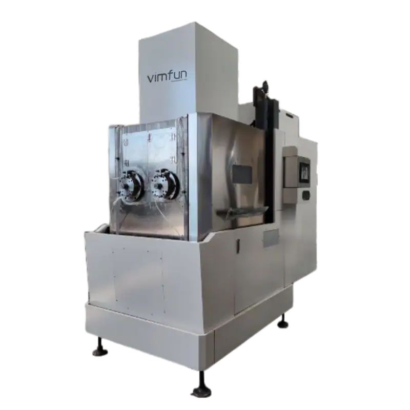
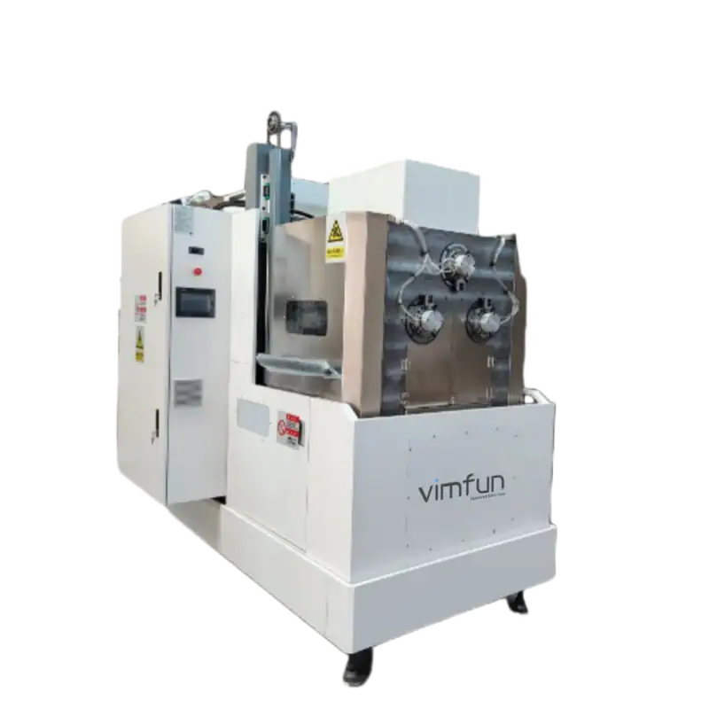
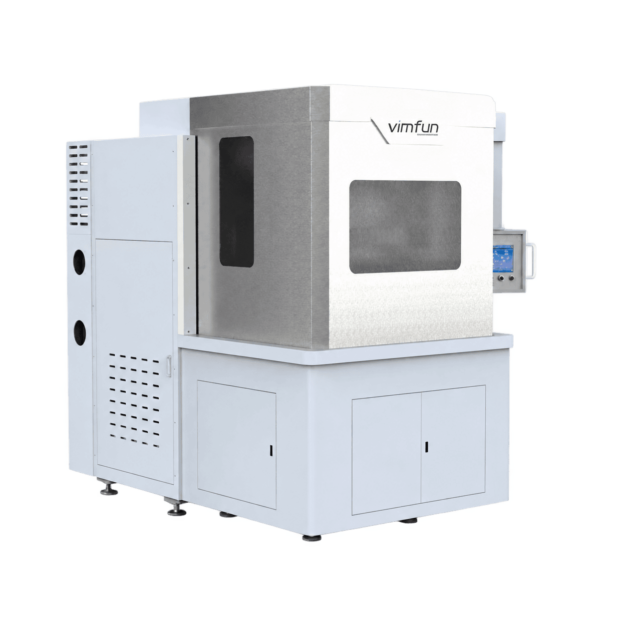
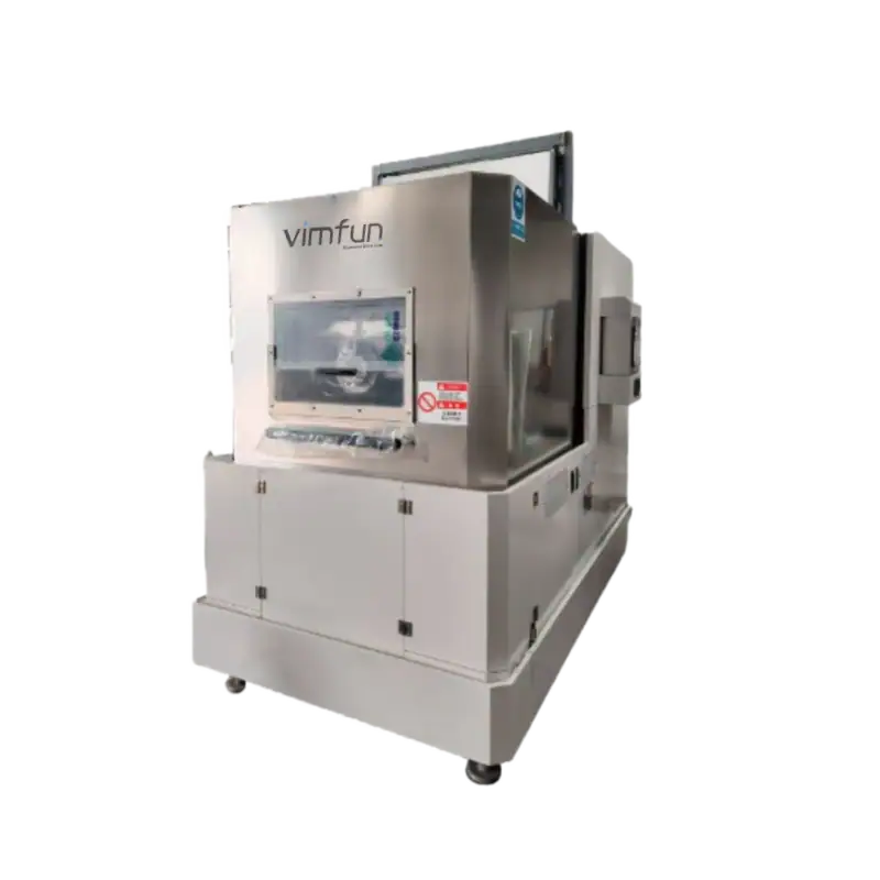
Vimfun is a Chinese manufacturer specializing in complete equipment solutions for semiconductor wafer manufacturing. Our portfolio covers the full process chain — from crystal growth to polished wafer.
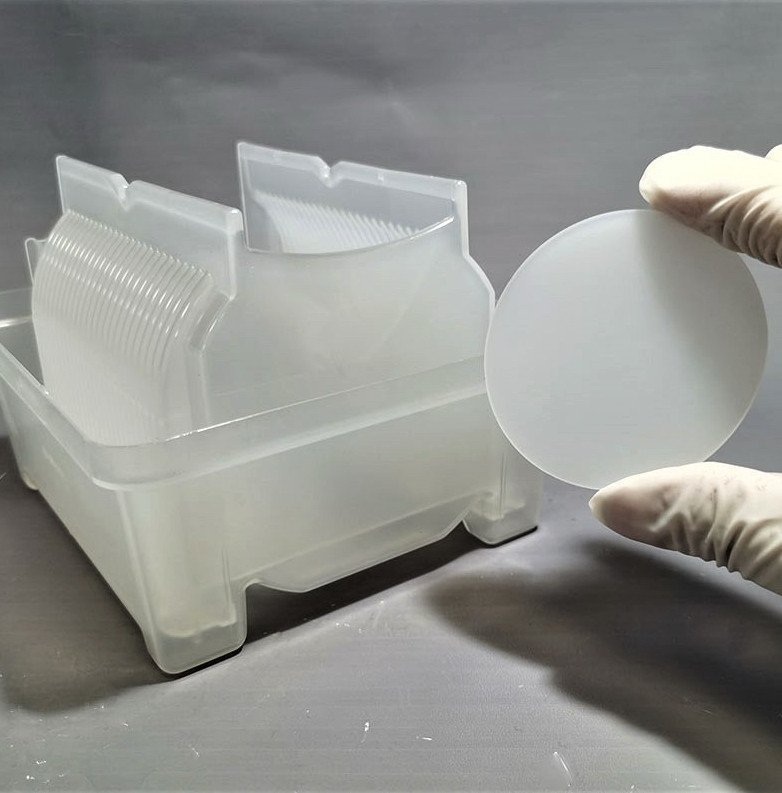
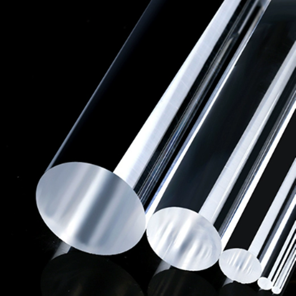
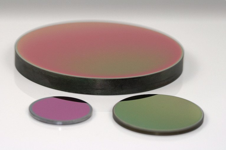
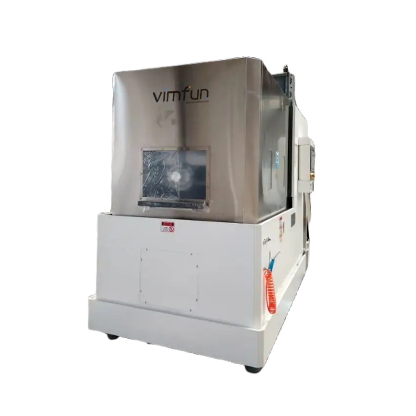
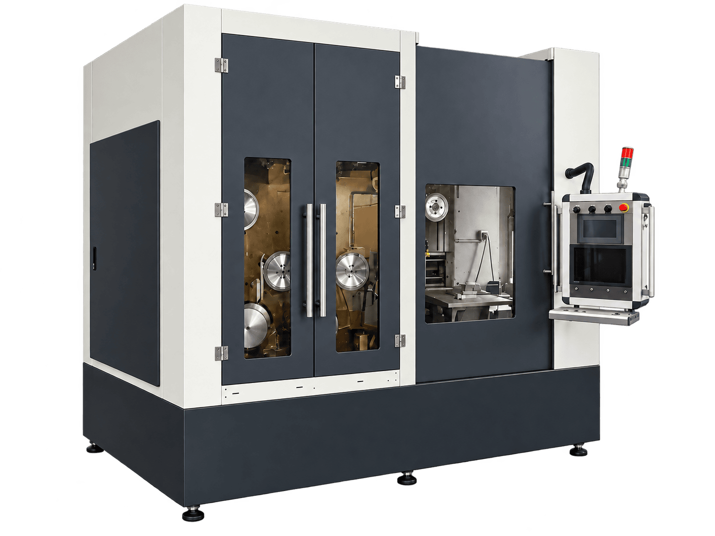
Crystal growth furnaces using Continuous Czochralski (CCz) and Kyropoulos methods produce ultra-pure Si, sapphire, and Ge ingots. Multi-wire diamond saws slice these ingots into wafers with ultra-low kerf loss and chip-free edges. Double-sided lapping and polishing machines deliver sub-micron flatness and sub-nanometer surface roughness. We serve silicon ingot producers, SiC and sapphire substrate manufacturers, advanced ceramic processors, and infrared optics foundries worldwide.
무료 샘플 컷
공작물과 도면을 보내주시면 무료 샘플 컷을 제공합니다.
머신 설계
특정 절단 요구 사항에 맞는 기계 설계
소모품
원활한 기계 작동을 위한 모든 필수 소모품 제공
OUR EQUIPMENT PORTFOLIO
Equipment for Every Stage of Wafer Manufacturing
From single crystal growth to mirror-finished wafers, our equipment portfolio covers every stage of semiconductor manufacturing. Below, machines are organized by process stage — each engineered for specific material hardness, workpiece geometry, and throughput requirements.
- 방법: 연속 초크랄스키 (CCz) / H-MCZ
- 최대 용량: 1000kg (맞춤 가능)
- 최대 직경: 300 mm / 12 인치
- 균일성: < 6.0% 비저항 (RRG)
- 방법: 연속 초크랄스키 (CCz) / H-MCZ
- 최대 용량: 1000kg (맞춤 가능)
- 최대 직경: 300 mm / 12 인치
- 균일성: < 6.0% 비저항 (RRG)
INDUSTRIES WE SERVE
Trusted by Semiconductor Manufacturers Worldwide
Our equipment serves silicon ingot producers, SiC and sapphire substrate manufacturers, and ceramic processors across Asia, Europe, and North America. Typical applications include high-volume wafer production for power semiconductors, LED substrates, RF devices, and advanced ceramic packaging — delivering ultra-low kerf loss, sub-micron flatness, and stable throughput.
Silicon ingot slicing
Slicing monocrystalline Si ingots into wafers with ultra-low kerf loss. Compatible with 6-inch to 12-inch diameters.
기계 확인
Germanium Wafer
Slicing CZ-grown germanium ingots into wafers for SiGe applications, solar cells, and detector substrates.
기계 확인
GaN & GaAs Substrate
Precision cutting of compound semiconductor crystals for RF, power, and optoelectronic device manufacturing.
기계 확인
Sapphire Wafer for LED & MEMS
Slicing C-plane and A-plane sapphire ingots into ultra-thin wafers for LED epitaxy, MEMS, and protective covers.
기계 확인
Piezoelectric Ceramic Slicing
Ultra-thin slicing of PZT, lithium niobate, and quartz crystals for sensors, transducers, and SAW filters.
기계 확인
Ultra-Thin Wafer (≤0.2mm)
Specialized SOM2-600S for ultra-thin wafer production where kerf loss control is critical.
기계 확인
SPECIALTY EQUIPMENT
For Permanent Magnet Manufacturing
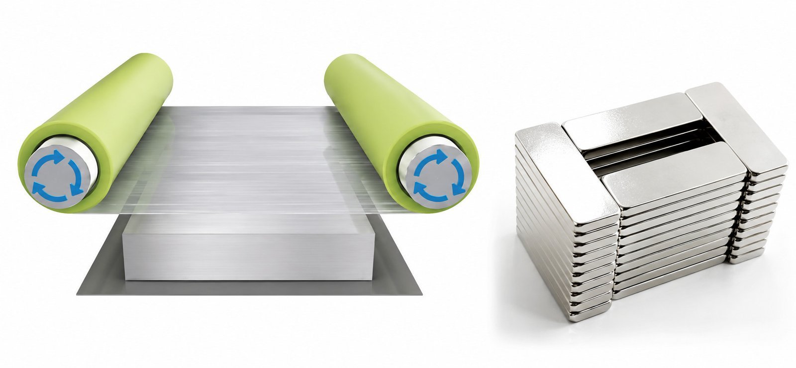
Beyond semiconductor wafers, Vimfun manufactures specialized arc-form grinding machines for high-volume permanent magnet (NdFeB) motor magnet production. For our complete permanent magnet processing portfolio, please visit our dedicated site.
회사 소개
커팅기가 더 나은 이유
딱딱하고 부서지기 쉬운 재료를 절단하는 데 다년간의 경험을 바탕으로 단순한 기계가 아닌 완벽한 절단 솔루션을 제공합니다. 당사의 장비는 매우 낮은 커프 손실, 프로그래밍 가능한 모션 제어, 깨끗한 절단 표면, 유연한 구성 옵션이 특징입니다. 전 세계적인 지원과 실제 성공을 바탕으로 고객이 더 스마트하고, 더 빠르고, 더 깨끗하게 절단할 수 있도록 돕습니다.

🔹 칩 없는 엣지 품질
🔹 매우 매끄러운 표면 마감
🔹 커프 손실 최소화
🔹 낮은 절단 스트레스
🔹 얇고 단단한 소재 지원
🔹 클린룸 호환 작동
뉴스 및 인사이트
전문가와 함께 앞서 나가세요
광학 재료 가공, 절단 기술 및 애플리케이션별 과제에 대한 심층적인 기사를 살펴보세요.