The first question we get from most buyers is direct: “Can your crystal growing furnace handle the material we need?” It’s the right question. Silicon, germanium, gallium arsenide, and compound semiconductors each demand different thermal environments, atmosphere control, and pulling mechanics — one furnace design does not cover them all.
This page walks through which crystal growing furnace materials our systems support, what each material needs to grow successfully, and which industries typically source each one. If you’re evaluating a furnace for a specific production line, use this as your starting point.
Why Material Choice Drives Furnace Design
Crystal growing furnace materials fall into three broad families, and each family has design requirements that carry through the entire furnace:
- Melting temperature — Silicon melts at 1414 °C; germanium at 938 °C; GaAs at 1238 °C. This determines heater design, insulation, and crucible material.
- Atmosphere requirements — Some materials need inert gas (argon); others need vacuum or reducing atmospheres.
- Pulling mechanics — Diameter, growth rate, and rotation vary widely between materials.
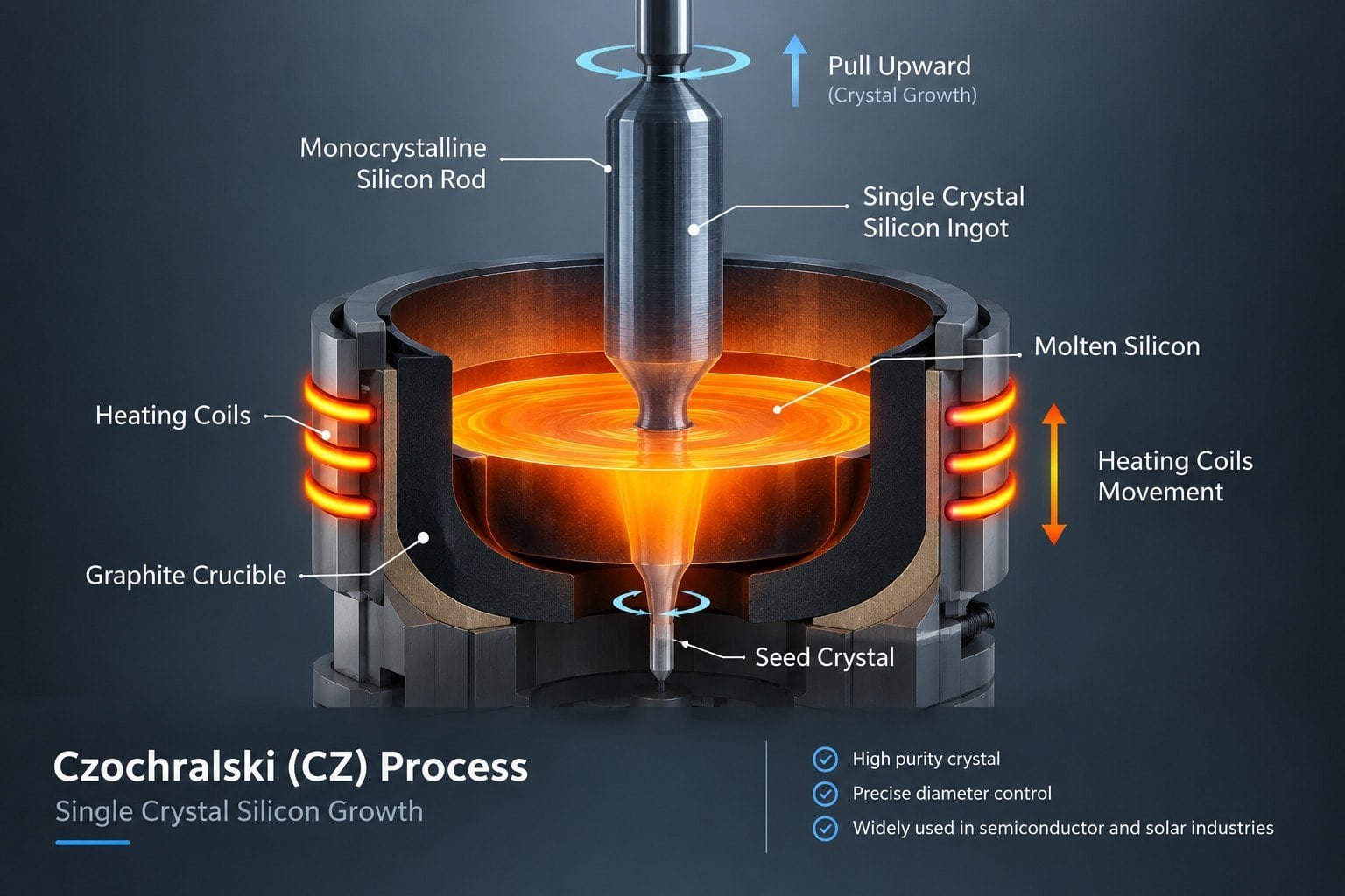
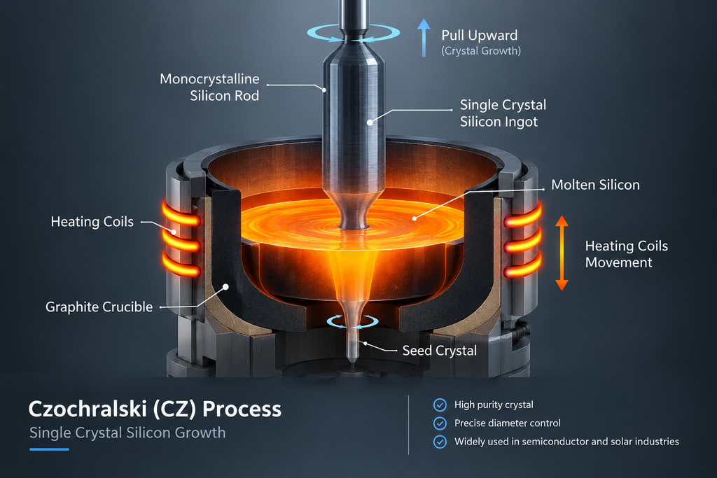
A furnace optimized for silicon won’t produce quality germanium crystals without significant modification. That’s why we build dedicated furnace configurations for each major material rather than trying to sell one system as universal. To understand the underlying crystal growth process, our how it works page covers the CZ (Czochralski) method that all these material families rely on.
Silicon — The Foundation of Semiconductors
Silicon remains the most-produced crystal growing furnace material by volume worldwide. Global silicon wafer demand continues to grow steadily, driven by chip production, solar photovoltaics, and sensors.
Where silicon crystal goes:
- Integrated circuit wafers (200 mm and 300 mm)
- Solar cell substrates (monocrystalline PV)
- MEMS sensor bases
- Power semiconductor substrates
What silicon growth demands:
- Stable ultra-high temperature above 1414 °C
- Argon atmosphere with strict oxygen control
- Precise pull rate control (typically 1.5–2.0 mm/min for large ingots)
- Multi-zone temperature uniformity (±0.5 °C matters)
Our silicon-focused furnace configurations support diameters from 6 inches up to 12 inches, with continuous CZ (CCZ) options for high-throughput production lines. The 12-inch MCZ crystal puller и CCZ-1600 continuous silicon puller are our two most-requested silicon systems.
Who typically buys silicon growth systems from us: Semiconductor foundries scaling production, solar cell manufacturers, and R&D labs evaluating new dopant profiles. If you’re producing wafers, silicon is where most conversations start.
Germanium — Precision Optics and Space Applications
Germanium is a quieter market than silicon, but it commands significantly higher margins. Our germanium crystal growing furnace materials serve a small, specialized customer base with strict quality requirements.
Where germanium crystal goes:
- Infrared optics (thermal imaging, night vision)
- Space-grade detectors (satellite payloads, IR astronomy)
- Fiber optic components
- Solar concentrator cells for space
What germanium growth demands:
- Lower melting temperature (938 °C) — different heater architecture than silicon
- Very tight thermal gradient control (germanium is more sensitive to stress cracking during cooling)
- High-purity graphite crucibles
- Dedicated pull mechanics — reusing silicon equipment produces defective germanium ingots
Germanium is one of those crystal growing furnace materials where trying to save money with a general-purpose furnace almost always backfires. The material is expensive enough per kilogram that yield loss on defective ingots dwarfs any furnace cost savings. Our Ge growth furnace configurations are purpose-built for this reason. For downstream processing considerations, our germanium blank cutting article covers how the wafer prep chain integrates with growth.
Who typically buys germanium growth systems from us: Defense optics manufacturers, space payload integrators, and specialty infrared component producers. Volumes are small, unit values are high.
Gallium Arsenide — The Compound Semiconductor Backbone
Gallium arsenide (GaAs) is the workhorse of compound semiconductors. Demand has grown alongside 5G wireless infrastructure, LED lighting, and semiconductor laser applications. Among compound crystal growing furnace materials, GaAs is by far the highest-volume category we support.
Where GaAs crystal goes:
- 5G RF front-end chips
- Power amplifiers for wireless base stations
- LED chips (high-brightness applications)
- Semiconductor lasers (fiber optic communications, industrial lasers)
- Photovoltaic cells for concentrator PV
What GaAs growth demands:
- Careful arsenic pressure control during melt (arsenic evaporates aggressively at melt temperature)
- Sealed growth chamber with pressure regulation
- Boron oxide encapsulant (LEC method) or vertical gradient freeze (VGF) approach
- Precise thermal gradient management to prevent dislocation formation
GaAs sits in a market segment where both semiconductor fabs and defense contractors buy. Growth systems for GaAs are typically more complex than silicon systems because of the arsenic pressure requirements, and lead times are correspondingly longer.
Who typically buys GaAs growth systems from us: Wireless infrastructure equipment makers, LED chip manufacturers, laser diode producers, and specialty compound semiconductor foundries.
Other Crystal Growing Furnace Materials
Beyond the big three, our furnaces support several smaller-volume but strategically important materials:
- Indium phosphide (InP) — High-frequency and photonic devices; fiber optic laser sources
- Lithium niobate (LiNbO₃) — Nonlinear optics, surface acoustic wave (SAW) filters, integrated photonics
- Sapphire (Al₂O₃) — LED substrates and specialty optical windows (grown via Kyropoulos method; see our sapphire growth furnace configurations)
- Карбид кремния (SiC) — Growing rapidly for power electronics, but requires PVT (physical vapor transport) rather than melt growth
- Lithium tantalate (LiTaO₃) — Optical waveguides and pyroelectric detectors
If your material isn’t on this list, contact us. We regularly build custom furnace configurations for specialty materials. Our custom crystal growing furnace page covers how the design consultation works.
Some materials — silicon carbide is the clearest example — are shifting the industry away from traditional melt-growth furnaces entirely. Buyers evaluating SiC should factor this into equipment purchasing decisions rather than assuming a silicon-style CZ furnace will meet their needs.
Material-to-Furnace Selection Reference
For buyers cross-referencing production plans against equipment options:
| Материал | Melting Point | Typical Growth Method | Common Application | Recommended Furnace Type |
|---|---|---|---|---|
| Кремний (Si) | 1414 °C | CZ / MCZ / CCZ | IC wafers, solar, sensors | Печь для выращивания кремния / MCZ / CCZ |
| Германий (Ge) | 938 °C | CZ (dedicated) | IR optics, space detectors | Печь для выращивания германия |
| GaAs | 1238 °C | LEC / VGF | 5G, LEDs, lasers | GaAs-configured CZ with sealed chamber |
| Sapphire (Al₂O₃) | 2053 °C | Киропулос | Подложки для светодиодов | Sapphire Growth Furnace |
| InP | 1062 °C | LEC | Photonics, high-freq | Compound semiconductor CZ |
| LiNbO₃ | 1257 °C | CZ | SAW filters, photonics | Oxide crystal CZ |
| SiC | (sublimes) | PVT | Power electronics | Not CZ — separate PVT system |
For temperature uniformity requirements across these materials, our temperature control page covers how multi-zone systems maintain the ±0.5 °C stability that most of these materials demand.
What to Tell Us When You Contact
The fastest way to get a useful quote is to send three pieces of information:
- Материал — Silicon, germanium, GaAs, or specify your compound
- Target crystal dimensions — Diameter and length range
- Production volume — Ingots per month or per year
From those three inputs, we can recommend a specific furnace configuration and provide a preliminary quote. If your requirements fall outside our standard configurations, we’ll flag that and start a custom design conversation.
For a broader look at how to evaluate crystal growing furnace materials against your production plan, our main crystal growing furnace page covers the full system overview.
Tell us your material and application. We’ll help you find the right furnace for it.
ЧАСТО ЗАДАВАЕМЫЕ ВОПРОСЫ
Q: Can one crystal growing furnace handle multiple materials?
A: In principle yes for R&D-scale multi-material work, but for production-grade quality, we recommend dedicated furnaces per material family. Trying to run silicon and germanium in the same furnace typically compromises yield on both.
Q: What’s the lead time for a new furnace?
A: Silicon and germanium standard configurations: 3–5 months. GaAs and custom compound furnaces: 5–7 months. Sapphire Kyropoulos furnaces: 4–6 months. Times vary with customization depth and current production queue.
Q: Do you support both R&D and production-scale customers?
A: Yes. Smaller diameter furnaces (2–4 inch) are common for research labs; production furnaces run 6, 8, 12, and larger diameters. We build both.
Q: Can you retrofit an existing furnace for a different material?
A: Usually not economically. The heater, crucible geometry, and atmosphere systems are material-specific enough that new furnace purchase is typically cheaper than conversion.
Q: What about silicon carbide?
A: SiC uses physical vapor transport (PVT), not melt growth. That’s a separate equipment category from CZ furnaces. Contact us for SiC options.