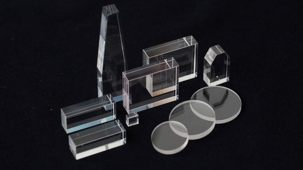
Semiconductor substrate materials such as silicon carbide (SiC), sapphire, and gallium arsenide are fundamental to advanced electronics, optoelectronics, and power devices. These materials are hard, brittle, and sensitive to mechanical stress, making handling, cutting, and processing a significant engineering challenge.
Their physical properties—high hardness, low fracture toughness, and low plastic deformation—mean that even small mechanical impacts can cause microcracks or chipping. Therefore, the choice of cutting technology, tooling, and process parameters is critical in ensuring wafer quality and maximizing yield.
Key Challenges in Handling Hard and Brittle Semiconductor Substrate Materials
Brittle Fracture and Microcracks
Brittle substrates have limited fracture toughness. During slicing, grinding, or polishing, mechanical forces must be carefully controlled. Otherwise, microcracks can form and propagate during later stages of wafer fabrication.
In high-volume semiconductor manufacturing, microcracks directly affect:
- Device reliability
- Surface integrity
- Yield loss
Precision cutting systems aim to minimize subsurface damage while maintaining processing efficiency.
Thermal and Mechanical Stresses
Cutting hard and brittle semiconductor substrate materials generates heat and stress. Uneven temperature distribution or excessive force may lead to:
- Kantenabsplitterungen
- Delamination
- Oberflächenrauheit
Advanced cutting techniques, including diamond wire saws and laser slicing, reduce stress concentration while ensuring consistent wafer thickness.
Kerf Loss and Material Utilization
Hard substrates are expensive. Efficient material utilization is critical. Kerf width, the material removed during slicing, directly impacts the number of wafers per ingot.
Modern precision techniques can reduce kerf width to around 0.4 mm for hard materials, improving cost efficiency without compromising wafer quality.
Cutting Technologies for Hard and Brittle Semiconductor Substrate Materials
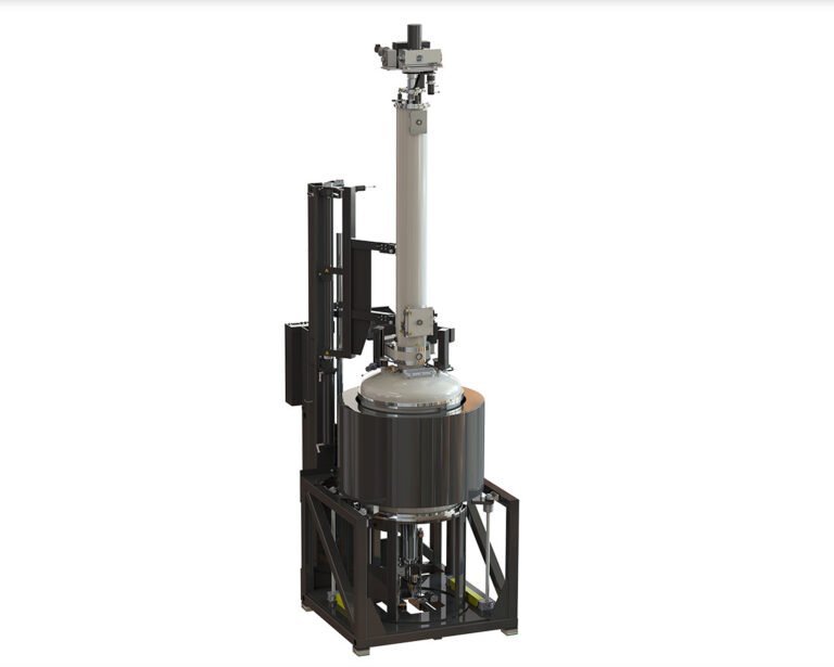
Diamond Wire Sawing
Diamond wire saws are widely used for slicing hard semiconductor substrates due to their high precision, low kerf loss, and minimal surface damage.
Key parameters:
- Wire speed: up to 80 m/s
- Wire tension: 150–250 N
- Kerf width: 0.35–0.45 mm
Advantages include reduced subsurface cracks, improved surface finish, and stable processing for brittle materials.
Laser schneiden
Laser cutting offers anon-contact method for slicing brittle semiconductor substrate materials. It is particularly useful for thin wafers or complex shapes.
Zu den Vorteilen gehören:
- Geringere mechanische Belastung
- Hohe Schnittpräzision
- Ability to process hard substrates that are challenging for conventional saws
Limitations include thermal effects, which require careful process control to avoid microcracking.
Ultrasonic and Hybrid Cutting Methods
Emerging hybrid methods combine mechanical and ultrasonic vibration to reduce cutting force. This minimizes crack formation in brittle substrates while maintaining productivity.
Ultrasonic-assisted cutting can achieve higher surface quality and lower tool wear for hard semiconductor substrate materials.
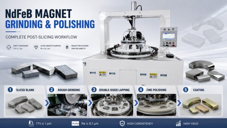
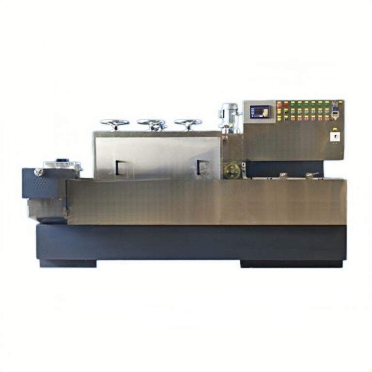
Surface Quality and Post-Processing
Even with advanced cutting, wafers often require:
- Grinding
- Lapping
- Polieren
High-quality cutting reduces post-processing time and improves wafer flatness, surface smoothness, and thickness uniformity. This is essential for downstream processes such as photolithography and device packaging.
Industrial Applications of Hard and Brittle Semiconductor Substrate Materials
Power Electronics
Silicon carbide (SiC) substrates are widely used in high-power electronics. Their high thermal conductivity, wide bandgap, and hardness require specialized semiconductor substrate materials handling and slicing technologies.
Optoelectronics and LEDs
Sapphire substrates are common in LED production. Diamond wire saws and precision grinding machines are critical for producing defect-free wafers with minimal chipping.
MEMS and Sensors
MEMS-Bauteile verwenden oft Wafer aus Galliumarsenid oder Silizium auf Isolator. Präzises Schneiden von harten semiconductor substrate materials gewährleistet Gerätegleichmäßigkeit und reduziert Nachbearbeitungskosten.
Wichtige technische Parameter
Schneidgeschwindigkeit
Die Optimierung der Schnittgeschwindigkeit gleicht die Materialabtragsrate mit der Oberflächenqualität aus. Zu schnell kann Risse verursachen; zu langsam reduziert die Effizienz.
Werkzeugspannung und Vorschub
Eine richtige Drahtspannung und Vorschubgeschwindigkeit sind unerlässlich, um Schnittbahnen zu stabilisieren und Brüche zu verhindern.
Kühlung und Späneentfernung
Ein effektiver Kühlmittelstrom entfernt Späne, verhindert Verstopfungen und erhält die thermische Stabilität während des Schneidens, was die Oberflächenqualität und Werkzeuglebensdauer verbessert.
Externe Ressourcen
Zum Weiterlesen:
- ScienceDirect – Wafer-Zerteilen und Substratmaterialien
- ThomasNet – Halbleiter-Wafer-Zerteilen
- MDPI – Laserschneiden von Siliziumwafern
FAQ: Harte und spröde Halbleiter-Substratmaterialien
F1: Was sind harte und spröde Halbleiter-Substratmaterialien?
A1: Materials such as SiC, sapphire, and GaAs, characterized by high hardness and low fracture toughness.
F2: Why are they difficult to process?
A2: Their brittleness makes them prone to microcracking and surface damage under mechanical stres
F3: How is material utilization optimized?
A3: By reducing kerf width during slicing and using precision cutting techniques.