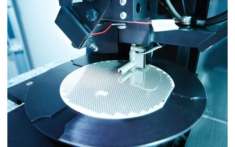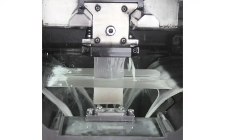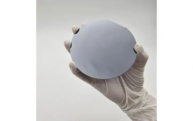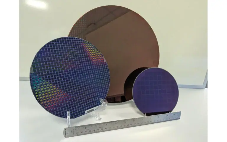
인듐 포스파이드(InP) 웨이퍼 슬라이싱
InP wafer slicing requires clear material identification, orientation and finishing allowance. Prepare a trial with traceable geometry and inspection.
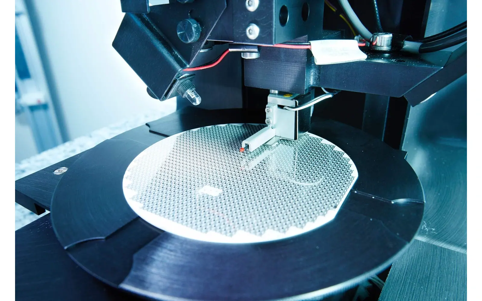
InP wafer blanks need a documented plane and enough stock for the receiving process. A visually clean slice is not evidence of orientation, electrical properties or subsurface condition. Define which of those features the trial will measure before sending the crystal.
An indium phosphide wafer is the output of a material-specific substrate route, not evidence that another semiconductor recipe is suitable. Start with the supplied InP stock, orientation and required blank geometry; select a compatible mounting and separation process, then evaluate released blanks and their finishing allowance. The equipment discussion here is a trial framework, not a claim of a qualified InP production recipe.
The InP wafer request should also settle support and release. If a thin blank is damaged during detachment, changing the saw setting may address the wrong stage. Keep inspection before and after release connected to the same slice identity.
Vimfun SOM200 explicitly lists indium phosphide in its material applications. For an InP wafer enquiry, that is a starting point for evaluating the stock and blank requirement, not proof of electrical quality, orientation retention or final surface acceptance.
Define the InP Wafer Requirement
Indium phosphide is a compound semiconductor, not another name for silicon or germanium. Identify the supplied crystal, its lot and the required plane. Include the available grade information from the material supplier and the intended receiving process.
그만큼 indium phosphide reference provides general material background. For an equipment decision, use the actual certificate and drawing as the authority. A photograph of a shiny wafer cannot verify composition, orientation or its functional suitability.
What will the saw trial actually establish?
A saw trial can establish measured geometry and observed condition within its stated scope. It does not automatically verify electrical properties, crystal defects or subsequent device performance. Assign each acceptance question to the responsible process and test method.
For an InP wafer, the output drawing should identify diameter or outside dimensions, blank thickness, reference plane and any orientation feature that must survive machining. List the defects relevant to the next operation rather than asking only for a visually clean surface.
If the stock is experimental or has unknown properties, disclose that before the trial. The result can still answer a limited mechanical question, but it should not be promoted as a general production capability for every InP grade.
Preserve the Crystal Reference through Preparation
Cropping and mounting can remove or obscure the original reference information. Identify how the desired plane is established and transferred to the fixture before machining. The outside shape of the stock is not necessarily the desired crystal datum.
An InP wafer trial should retain the lot, orientation record and slice identity. If the material is subdivided, document which pieces correspond to each section. This is especially useful when the receiving team investigates variation across the original crystal.
Record alignment checks and any authorized change in setup. A thickness trend found later is easier to interpret when the reference and mounting history are available.
Can the blank survive detachment?
The workpiece needs support as the cut develops and the blanks become separated. Fixture design should consider the final stage as well as initial rigidity. Where bonding is used, compatibility and release must follow an approved process for the actual material.
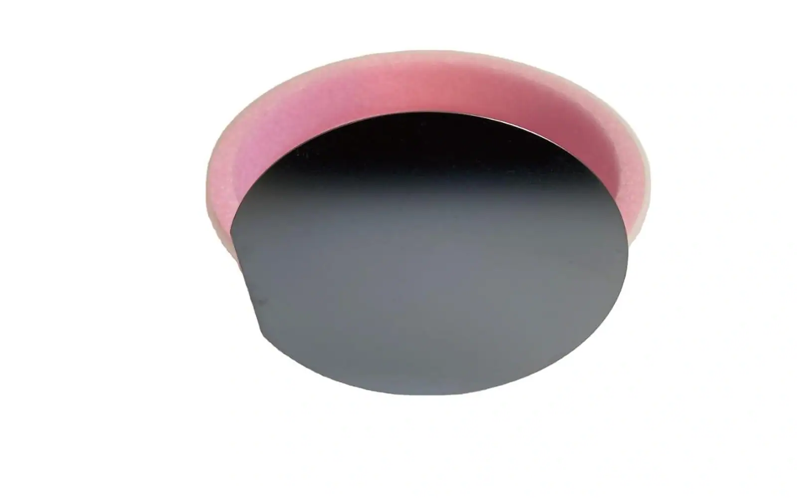
For an InP wafer request, include how the samples will be detached, carried and packaged. Thin blanks should not arrive at an improvised handling step after an otherwise successful cut. Keep the intended release procedure within the trial scope if its suitability is still uncertain.
Inspect accessible features before release and again afterward. That helps locate the stage at which defects appear instead of automatically assigning every final chip to the saw.
Select the Cutting Arrangement by the Actual Task
Repeated parallel substrates and an individual research section have different production objectives. Consider workpiece geometry, thickness, orientation and the number of acceptable blanks required. A nominal machine envelope does not define the achievable condition of every material it can accommodate.
The site's germanium wafer cutting page provides related semiconductor cutting context. Germanium is a different material; its reported behaviour must not be used as an InP performance guarantee.
An InP wafer trial should therefore use representative stock and an agreed output specification. Do not transfer feed, wire or cleaning settings from a silicon demonstration without the appropriate material and equipment assessment.
The SOM200 introduction explicitly includes indium phosphide in its material application list. It also lists a 200 × 200 × 200 mm maximum workpiece and a 0.3–12 mm slice range. Those references permit a focused feasibility discussion; they are not measured InP yield or a qualification for the thinnest blank.
For an InP wafer, use three separate acceptance fields: thickness geometry, crystal orientation and material-specific condition. Name the method for each. If the supplier checks only the first, the other two remain unverified rather than implicitly accepted.
I'd prioritize a supported, traceable trial over an aggressive thinness demonstration. The pitfall is counting one intact InP wafer as proof that the planned batch can survive release and finishing. Return representative pieces in order, including rejected samples that help locate where the problem occurred.
Preserve the slice identity.
Budget Cutting and Finishing Separately
The effective cut removes stock between blanks. Later finishing can remove more material to achieve the required geometry and surface condition. Set the as-cut thickness with the receiving team, including the approved allowance for those later operations.
An InP wafer that is uniformly thinner than required may be unusable even if its surface looks good. Conversely, excessive thickness can increase finishing effort. Record target thickness and allowable variation separately rather than hiding both in the word “precision.”
Keep geometric estimates separate from accepted recovery. Count pieces after the agreed release and inspection steps, and record rejects and their reasons. A projected slice count is not measured production yield.
Use Material-Specific Handling Controls
Machining creates debris and involves cleaning and waste streams that require appropriate controls. Provide the material's handling documentation and have the responsible facility assess the actual operation. This article does not replace a safety data sheet or a qualified local procedure.
A CDC publication on occupational indium exposure provides background on the importance of exposure assessment. Its scope is not an operating instruction for a particular InP machining setup, and it does not justify assuming that every form of indium-containing material has identical exposure behaviour.
For an InP wafer trial, confirm handling, cleaning, waste and shipping arrangements before dispatch. Avoid improvising a chemical release or cleaning method from an unrelated crystal example.
Which defects will your receiving process inspect?
Thickness sampling, orientation verification, edge inspection and surface evaluation answer different questions. Define the method and process stage for each. A centre thickness reading does not establish uniformity, and visual inspection does not establish subsurface condition.
For an InP wafer, identify whether the receiving team needs a finishing trial or another material-specific examination. Return representative samples rather than only the best-looking blank. Preserve slice order when it helps explain the result.
If an acceptance feature is not measured, label it unverified. The report should distinguish what the saw supplier demonstrated from what the customer must qualify in its own process.
Define the Qualification Boundary with the Material Owner
Ask the material owner to identify what the sample represents. Record the material lot, supplied state and orientation information with the geometry. An inspection photograph cannot establish those properties, and an abbreviation on a tray does not replace a traceable material record.
For an InP wafer trial, divide acceptance into the features the machining supplier measures and the features owned by the receiving process. A dimensional report is valuable, but it should not imply that unmeasured material or device properties passed. Put open qualifications in their own column so they remain visible after the blanks are returned.
Agree handling requirements before choosing the mounting arrangement. The supplier and receiving site should use their approved material-specific controls and qualified procedures. This article is not a substitute for the site’s safety assessment or an invitation to choose cleaning chemistry from a generic cutting recipe.
Keep the release method connected to the blank drawing. Identify which faces carry locating information and which may be changed later. If release or cleanup removes a mark, transfer identity under the approved procedure before it is lost. A correctly dimensioned piece without an interpretable reference may not answer the research or production question.
The InP wafer inspection package should include the measured state. Retain any later correction history, sample selection and excluded pieces. A specially finished sample may demonstrate that one specimen can reach a receiver, but it should not silently represent the condition of every piece immediately after cutting.
When a result is unsatisfactory, classify the question before changing equipment. Was the geometry wrong, was the material identity incomplete, or did the receiver reject a feature outside the original inspection scope? These are different investigations. A single pass/fail label hides the information needed to decide the next test.
A useful follow-up trial changes one named uncertainty and keeps the others documented. The goal is a traceable blank that the receiving team can evaluate. It is not a broad claim that a catalogue material listing settles the entire qualification route.
| 결정 필드 | 유지할 증거 |
|---|---|
| Material ownership | Lot, supplied state and orientation record |
| Machining scope | Geometry and release condition actually measured |
| Receiving scope | Additional material/surface qualification and owner |
질문에 답하는 페이지 선택
This article answers: Which conditions can machining demonstrate without claiming material or device qualification? It does not replace the following equipment or application scopes.
| 귀하의 질문 | 관련 페이지 | 경계 |
|---|---|---|
| Need the germanium wafer cutting context? | germanium wafer cutting | 수신 작업에 대한 애플리케이션 또는 프로세스 컨텍스트 |
자주 묻는 질문
Does a catalogue application qualify an InP wafer?
No. An InP wafer trial must establish the conditions relevant to the actual sample and receiver. A material listing supports an equipment discussion; it does not certify every grade, reference transfer or final qualification requirement.
Can an InP wafer trial inherit an unreviewed silicon procedure?
Do not assume so. Obtain the material owner’s requirements and use the site’s approved handling and processing procedures. Similar blank geometry does not establish that materials share the same release, cleaning or acceptance conditions.
How should an unmeasured InP wafer property be reported?
Mark it as unverified and identify who will evaluate it. Keep that distinction in the returned report. A satisfactory dimensional result must not be expanded into an assertion that electrical, orientation or surface qualifications have all passed.
Make the Test Report Traceable
Request material identification, input dimensions, mounting photographs, cutting notes, interruptions, output count and inspection data. Keep rejected specimens where they can support a failure investigation. Note any adjustments made during the run and the samples affected.
An InP wafer trial is most valuable when it resolves a named uncertainty. A first cut may establish separation while leaving release, finishing or larger-scale behaviour pending. Define the next test around that remaining question instead of repeating a general demonstration.
Provide the InP identity and plane, mounted geometry, blank thickness and finishing allowance. Confirm material-specific handling and return arrangements with the responsible facility. Ask the report to separate dimensional checks from unmeasured properties and to preserve InP wafer sequence through release. Review the receiving-process result before treating the cut as qualified production.