실리콘 웨이퍼는 어떻게 절단되나요? 잉곳에서 완성된 웨이퍼까지
Preparation, wire cutting and release: keep the blank target and inspection plan connected.
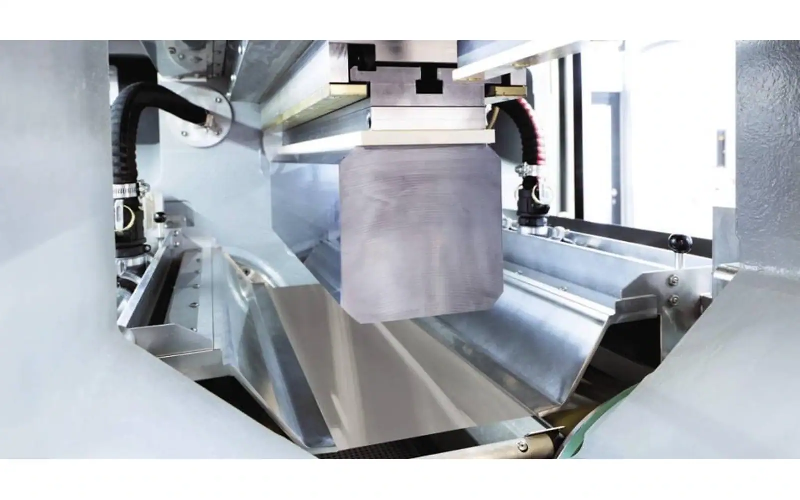
How are silicon wafers cut without leaving the finishing team an unusable blank? Establish the crystal plane, mount the ingot against a documented reference, divide it at the required spacing and inspect the slices after release. The as-cut target must include the stock that finishing will remove.
The difficult part is preserving that chain. A correct guide pitch will not rescue an ingot mounted at the wrong angle, and an intact batch can still be damaged during detachment. The practical answer to “how are silicon wafers cut” therefore includes fixture alignment and release, not only the running wire.
Vimfun SOM200 lists silicon among its slicing applications. That identifies a machine concept for review, not a silicon-wafer qualification: the crystal plane, blank target and receiving inspection still have to be specified for the trial.
How Are Silicon Wafers Cut in a Controlled Process?
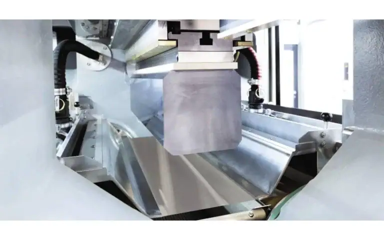
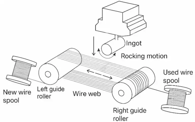
The saw removes material along planes that divide the ingot into blanks. In multi-wire cutting, a guided wire web creates repeated cutting positions so that multiple slices can be formed within one setup. A separate setup may be more appropriate for an individual research section or a special orientation requirement.
그만큼 wafer overview distinguishes the substrate from the later devices built on it. That distinction matters here: separating a silicon blank does not establish its final surface quality, cleanliness or suitability for device fabrication.
Identify the Material before Planning the Cut
Material documentation should travel with the ingot. Record crystal form, lot identification, intended wafer orientation and any known sections excluded from use. Do not infer these attributes from a glossy surface or a supplier photograph. A correct cut on the wrong starting material is still the wrong product.
When teams ask how are silicon wafers cut, they often focus immediately on the wire. The reference plane should be settled first. The drawing and orientation documentation need to identify how the desired wafer plane relates to the ingot and how that relationship will be maintained through mounting.
Record the input dimensions as measured, including the portion available for fixture attachment and end allowances. An equipment capacity check must consider the mounted assembly, not only the bare crystal diameter.
Which thickness should the saw actually produce?
Translate the final wafer requirement into a blank specification. Subsequent surface processing may remove material, so the saw target must reserve the approved finishing allowance. Define whether the requested thickness is nominal, average or a limit applied to every measured point.
There are two questions hidden inside “how are silicon wafers cut”: how a section is physically separated, and how its geometry is controlled. The second requires a measurement plan. Select the sampling locations and edge exclusion before the trial, then use the same method for all compared configurations.
For the application context, review 실리콘 잉곳 슬라이싱. The material-specific discussion should support the drawing and acceptance sheet rather than replace them with an assumed universal tolerance.
Prepare and Mount the Ingot
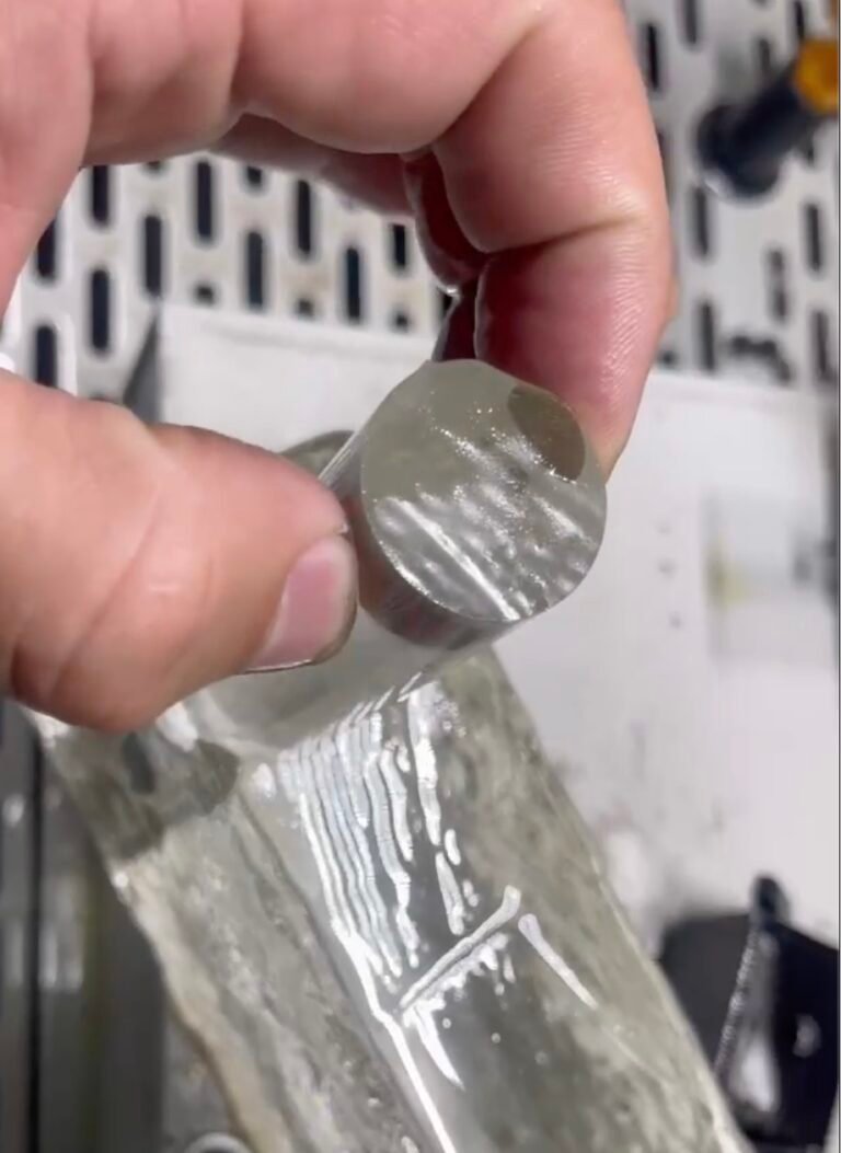
Cutting silicon wafers starts with an oriented, prepared ingot, not with a finished wafer on a dicing chuck. Silicon ingot cutting divides this stock into blanks: the guides position a moving wire web, the workpiece advances through that web, and abrasive contact removes material between the retained slices. The operator preserves support through separation before releasing and cleaning the blanks. This explains how to cut silicon wafer blanks from bulk stock; cutting a finished wafer into chips is a different operation.
Preparation makes the workpiece locatable and supportable. Confirm that the fixture does not obscure required reference marks or prevent the intended movement. The operator must be able to verify alignment without relying on a later thickness result to reveal an error.
A mounting plan also includes separation after cutting. If the process uses bonding, the release method should be qualified for the material and support system. State how thin blanks will be held while attachment material is removed and how slice order will be preserved.
How are silicon wafers cut consistently when mounting varies from batch to batch? Start by making mounting a recorded process. Keep the fixture identification, locating surfaces, relevant setup checks and photographs with the work order. That makes a thickness trend easier to investigate.
Use a setup sheet that identifies the intended plane, the locating feature and the inspection datum. Those are three separate descriptions, even when one face serves more than one purpose. A fixture photograph should show the relevant mark and support; a close-up of the wire cannot establish alignment.
When explaining how are silicon wafers cut, distinguish groove pitch from retained thickness. The pitch allocates the repeating interval, while the effective cut removes part of it. Recording only the nominal pitch leaves the receiving team without an explanation for a thickness difference.
I'd mark the first slice and preserve sequence through release. If thickness drifts along the batch, the ordered measurements are much more useful than a bag of selected good pieces. How are silicon wafers cut consistently? Make the datum and sequence reproducible before trying to shorten the cycle.
Pitch is not retained thickness.
What should be checked before the wire touches silicon?
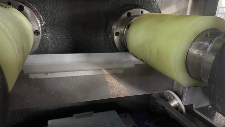
A wire web must match the intended slice spacing and be compatible with the selected cutting system. Groove geometry, tracking, consumable condition and alignment should be checked using the equipment procedure. A visible web alone does not show that every cutting position is correctly established.
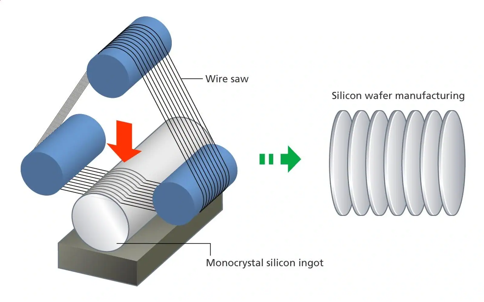
그만큼 multi-wire operating principle explains the repeated-line arrangement. For selection of an overall 웨이퍼 슬라이싱 기계, compare the actual workpiece and production objective rather than equating machine size with finished-wafer capability.
How are silicon wafers cut at the intended spacing? The guide arrangement establishes the repeated positions, while the effective cutting width and operating condition affect the retained blank. A nominal spacing is therefore not a substitute for measuring actual thickness after release.
Monitor Entry, the Main Cut and Exit
The cut changes as contact develops and as separation approaches completion. Support, fluid access and tool behaviour should be assessed over the entire cycle. A process that appears stable in the middle of the ingot may still create defects near entry or final release.
Record interruptions and visible changes during a trial. If an operator adjusts the process, note when the change occurred and which slice positions could be affected. Otherwise, inspection results may be averaged across different conditions without anyone recognizing the difference.
How are silicon wafers cut with minimal unplanned damage? There is no universal feed or wire recipe in this guide. Use the equipment procedure and a material-specific trial, then evaluate the output against the defined finishing route. Avoid borrowing settings from an unrelated crystal or machine.
Release and Clean without Mixing the Evidence
After the cut, retain support until the planned release procedure permits separation. Provide a suitable carrier and handling method. It is difficult to diagnose damage if slices are stacked loosely or their order is lost before inspection.
Inspect accessible features before release and again after cleaning. This establishes whether a defect appeared at the saw, during detachment or during handling. The cleaning method must follow the approved site process and material compatibility requirements.
When answering how are silicon wafers cut for a quality review, include these post-cut operations. A report ending at cycle completion omits a stage where accepted output can still be lost.
Can one thickness reading qualify a batch?
Thickness mapping, edge inspection and surface assessment answer different questions. A single centre measurement does not prove uniform thickness, and a clean-looking surface does not demonstrate the absence of subsurface damage. State which methods were actually used.
Compare the output with the as-cut acceptance sheet, then send representative material to the receiving operation. If a finishing trial is part of the project, keep its results separate so that removal allowance and damage clearance can be evaluated directly.
How are silicon wafers cut successfully in production? The strongest evidence is repeated accepted output from representative stock, measured by the same method. One selected blank establishes that a piece was produced, not that a stable batch capability has been demonstrated.
Use a Cut Plan That the Next Shift Can Follow
Write the cutting sequence as instructions for someone who did not attend the planning meeting. Identify the stock, the retained section and the reference used for mounting. A sketch that shows only the desired wafer is incomplete if it does not show how the operator locates that plane on the incoming ingot.
When asking “how are silicon wafers cut?”, keep setup approval distinct from output approval. Check the material identification and mounting reference before entry. Then inspect the released pieces under the agreed method. Passing the first check does not make the second redundant; a documented setup can still produce an output that requires investigation.
Name the person who may stop the trial when the workpiece or fixture condition differs from the drawing. An operator should not have to decide whether an undocumented material mark is optional. Resolve that discrepancy before it disappears in preparation or becomes difficult to trace after separation.
Retain enough stock for the receiving operation, but do not insert an arbitrary extra allowance to hide uncertainty. Ask the finishing team which surface condition and dimensional window it needs. If those requirements are not yet settled, record the trial as exploratory rather than presenting its blank target as a production specification.
The practical answer to “how are silicon wafers cut?” also includes release. Describe how the assembly is supported as slices become separate pieces, how their positions are retained and which measurements occur before cleaning. A cutting record that ends at the last wire pass cannot establish where later damage arose.
Use the same blank identity for photographs, inspection and finishing feedback. If samples are selected for further evaluation, record their positions instead of returning only the best-looking pieces. Selection is permissible; an undocumented selection changes what the sample can represent.
Before repeating the route, ask whether the incoming stock and receiver still match the approved trial. Changes in either can require a new setup assessment. The answer to “how are silicon wafers cut?” should make those differences visible without forcing the next engineer to reconstruct the job from operator memory.
| Decision field | Evidence to retain |
|---|---|
| Before entry | Material identity, plane and mounting reference |
| At separation | Slice order and support/release arrangement |
| At receipt | Blank window, inspection method and selection record |
질문에 답하는 페이지 선택
This article answers: What must be controlled from ingot identification through released blanks? It does not replace the following equipment or application scopes.
| 귀하의 질문 | 관련 페이지 | 경계 |
|---|---|---|
| Need the silicon ingot slicing context? | 실리콘 잉곳 슬라이싱 | 수신 작업에 대한 애플리케이션 또는 프로세스 컨텍스트 |
| Need the multi-wire operating principle context? | multi-wire operating principle | 수신 작업에 대한 애플리케이션 또는 프로세스 컨텍스트 |
| Need the wafer slicing machine context? | 웨이퍼 슬라이싱 기계 | 수신 작업에 대한 애플리케이션 또는 프로세스 컨텍스트 |
| Need the complete ingot-to-finished-wafer route? | wafering | Crystal growth through finished substrate production |
자주 묻는 질문
How are silicon wafers cut when finishing still removes stock?
The answer depends on the route. When finishing removes stock, the saw produces an intermediate target rather than the finished value. The question “how are silicon wafers cut?” must therefore be answered with the as-cut drawing and the subsequent removal requirement together.
How are silicon wafers cut to a measured blank target?
Guide geometry defines part of the setup, and inspection establishes the released blank condition. The released blank still needs the agreed thickness inspection. Keep nominal setup dimensions and measured output in separate report fields so that a dimensional trend can be investigated.
How are silicon wafers cut in a useful first trial?
It should demonstrate an identifiable batch of blanks that the receiving process can evaluate. Include orientation references, slice order, release condition and inspection results. A successful separation alone does not establish a production-ready silicon cutting route.
Prepare a Useful Trial Request
How are silicon wafers cut for your specified receiving process? Resolve that question with the material, blank drawing and inspection requirements below.
Supply material identification, input geometry, intended plane, blank thickness, finishing allowance and the defects that would make a slice unusable. Identify who will inspect the returned pieces and whether the team needs slice-order records.
The practical answer to “how are silicon wafers cut?” is a documented sequence: establish the reference, mount the ingot, verify the cutting arrangement, separate the blanks, release them safely within the approved procedure and measure them. Keeping those steps connected makes the result useful to the next operation and to the equipment decision.
Prepare one drawing showing the crystal plane, mounted envelope, blank thickness and finishing allowance. Before cutting, photograph the locating reference and check the guide arrangement under the machine procedure. After release, retain slice order and measure the agreed area. Use that baseline to answer how are silicon wafers cut successfully on your material, then investigate speed only after the blanks pass.