Overview of Semiconductor Wafer Manufacturing
Modern electronics—from smartphones and data centers to electric vehicles—depend on highly reliable semiconductor devices. At the foundation of these devices are semiconductor wafers, which serve as the substrate for integrated circuit fabrication.
Semiconductor wafer manufacturing involves a series of highly controlled industrial processes that convert raw crystalline materials into ultra-flat wafers suitable for microelectronic device fabrication.
Because semiconductor materials are brittle and extremely valuable, the production process requires advanced machining technologies capable of maintaining high precision while minimizing material waste.
For manufacturers, selecting appropriate slicing and cutting equipment plays a critical role in improving wafer yield and reducing processing costs.
What Is Semiconductor Wafer Manufacturing
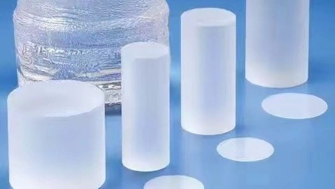
Semiconductor wafer manufacturing refers to the industrial process of producing thin, polished semiconductor substrates used in microchip fabrication.
The most common wafer materials include:
- Silicon (Si)
- Silicon carbide (SiC)
- Gallium arsenide (GaAs)
- Gallium nitride (GaN)
- Sapphire substrates
These materials are chosen based on their electrical, thermal, and mechanical properties.
The final wafers must meet strict engineering specifications such as:
- Thickness uniformity
- Flatness (TTV control)
- Surface roughness
- Crystal orientation accuracy
- Minimal subsurface damage
Even microscopic defects can reduce chip yield during photolithography and device fabrication.
Main Process Steps in Wafer Production
Although production methods vary depending on the semiconductor material, the overall workflow of semiconductor wafer manufacturing generally follows several major stages.
1. Crystal Growth
The first step is producing a high-purity single-crystal ingot.
Common crystal growth methods include:
Czochralski (CZ) Process
Widely used for silicon wafers in integrated circuit production.
Float-Zone (FZ) Method
Produces ultra-high purity silicon for power semiconductor devices.
Physical Vapor Transport (PVT)
Commonly used for silicon carbide crystal growth.
The resulting ingots can reach diameters of 200 mm, 300 mm, or larger depending on the application.
Precise thermal control is essential to prevent crystal defects and dislocations.
2. Ingot Shaping and Alignment
After crystal growth, the ingot undergoes mechanical preparation.
Typical operations include:
- Cylindrical grinding
- Orientation notch or flat creation
- Surface defect removal
These steps ensure correct crystal alignment before slicing the ingot into wafers.
3. Wafer Slicing
Wafer slicing is one of the most critical stages in semiconductor wafer manufacturing because it directly determines wafer thickness consistency and material utilization.
Common slicing technologies include:
- Inner diameter (ID) saws
- Multi-wire slurry saws
- Fixed abrasive wire saws
However, semiconductor materials are typically brittle and sensitive to mechanical stress. Conventional blade cutting methods may introduce defects such as chipping and microcracks.
For advanced semiconductor materials like silicon carbide, more precise cutting technologies are increasingly required.
Machining Challenges in Semiconductor Materials
Processing semiconductor crystals presents unique challenges for manufacturing engineers.
Brittle Material Behavior
Most semiconductor materials exhibit brittle fracture characteristics rather than plastic deformation during machining.
This can lead to:
- Edge chipping
- Surface microcracks
- Subsurface damage layers
These defects must be removed during lapping and polishing processes, which increases manufacturing cost and cycle time.
Kerf Loss and Material Cost
Kerf loss refers to the material removed during slicing.
Traditional cutting methods often generate wide kerfs, resulting in significant raw material waste.
For high-value materials such as silicon carbide or gallium nitride, reducing kerf loss is a major priority in semiconductor wafer manufacturing.
Surface Damage Control
The slicing process inevitably introduces surface and subsurface damage.
If the damage layer is too deep, additional polishing steps are required to restore wafer quality. This reduces throughput and increases production costs.
Therefore, manufacturers are increasingly adopting cutting technologies designed to minimize mechanical stress during slicing.
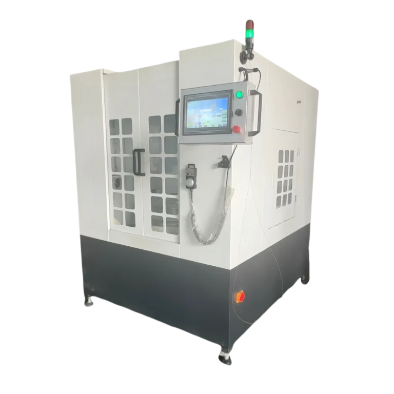
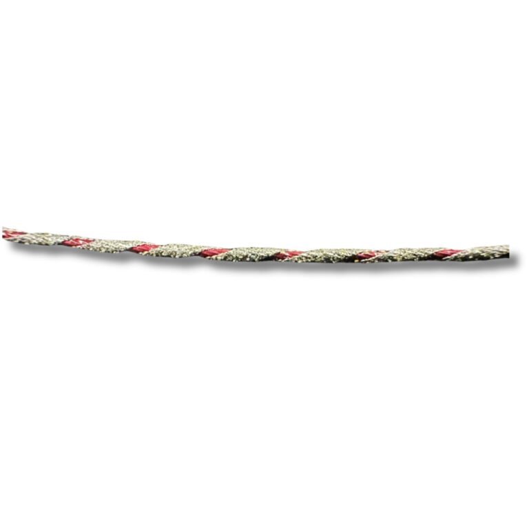
Endless Diamond Wire Cutting Technology
To improve cutting precision and material efficiency, advanced wire cutting technologies are being adopted across semiconductor industries.
One effective solution is the machine de découpe de fil diamanté sans fin, designed specifically for precision cutting of hard and brittle materials.
Working Principle
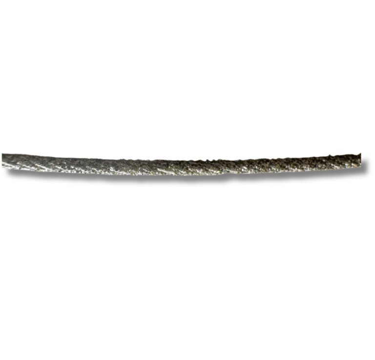
An endless diamond wire system uses a continuous loop of diamond-coated wire that moves at high speed while maintaining stable tension.
Typical machine parameters include:
- Wire speed up to 80 m/s
- Wire tension between 150–250 N
- Kerf width approximately 0.4 mm
The diamond abrasives grind the material during cutting rather than applying large mechanical forces like traditional blades.
This grinding mechanism significantly reduces the risk of brittle fracture during wafer slicing.
Engineering Advantages of Endless Diamond Wire Cutting
For engineers involved in semiconductor wafer manufacturing, endless diamond wire technology provides several key advantages.
Reduced Kerf Loss
A kerf width of approximately 0.4 mm allows higher material utilization compared with traditional slicing methods.
This is particularly beneficial when processing expensive semiconductor crystals.
Improved Surface Quality
The grinding action of diamond abrasives reduces edge chipping and microcracks.
As a result, wafers require less material removal during subsequent lapping and polishing processes.
High Cutting Precision
Stable wire tension between 150–250 N ensures consistent cutting conditions.
This improves wafer thickness uniformity and dimensional accuracy.
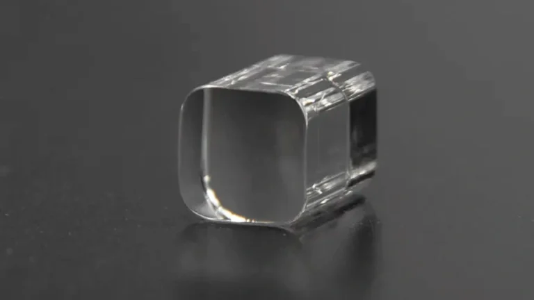
Suitability for Hard and Brittle Materials
Endless diamond wire systems are capable of processing materials such as:
- Silicon carbide (SiC)
- Saphir
- Gallium nitride (GaN)
- Optical crystals
- Advanced ceramics
These materials are increasingly used in high-power electronics and optoelectronic devices.
Applications industrielles
Precision wire cutting technologies are widely used in multiple high-tech manufacturing industries.
Typical applications include:
Production de plaquettes de silicium
Used for integrated circuits and logic devices.
Silicon Carbide Wafers
Critical for electric vehicles, power electronics, and renewable energy systems.
LED Sapphire Substrates
High-precision slicing for optoelectronic devices.
Optical Crystal Processing
Used in lasers, sensors, and photonic systems.
Advanced Ceramic Components
High-performance materials used in aerospace and electronics industries.
These applications require machining technologies capable of achieving tight dimensional tolerances and minimal surface damage.
Future Trends in Wafer Manufacturing
The semiconductor industry is rapidly evolving, placing new demands on wafer production technologies.
Several trends are shaping the future of semiconductor wafer manufacturing.
Larger Wafer Sizes
Increasing wafer diameter improves production efficiency but requires extremely precise machining equipment.
Wide Bandgap Semiconductor Materials
Materials such as SiC and GaN are becoming essential for next-generation power electronics and high-frequency devices.
These materials are significantly harder than silicon and require advanced cutting technologies.
Higher Surface Quality Standards
As semiconductor devices continue to shrink in size, wafer surface quality and thickness uniformity become increasingly critical.
FAQ: Semiconductor Wafer Manufacturing
Why is wafer slicing important in semiconductor production?
Wafer slicing determines the thickness uniformity, surface quality, and material utilization of semiconductor wafers. Poor slicing quality can lead to higher polishing costs and lower device yield.
Why are diamond wire cutting technologies used?
Diamond wire cutting provides high precision, narrow kerf width, and reduced mechanical stress, making it suitable for cutting brittle semiconductor materials.
Which materials are most difficult to cut?
Silicon carbide, sapphire, and gallium nitride are among the most difficult semiconductor materials due to their high hardness and brittle characteristics.
Conclusion
Semiconductor wafers form the fundamental building blocks of modern electronics. Producing these wafers requires highly controlled manufacturing processes and precision machining technologies.
Throughout semiconductor wafer manufacturing, wafer slicing plays a crucial role in determining material utilization, wafer quality, and overall production efficiency.
Advanced cutting solutions such as endless diamond wire technology offer significant advantages in processing brittle semiconductor materials. By reducing kerf loss, improving surface quality, and maintaining high cutting precision, these systems help semiconductor manufacturers achieve higher yields and more efficient production.