Semiconductor wafer cutting is a critical process in semiconductor manufacturing, where large single-crystal ingots are sliced into thin wafers used for integrated circuits, sensors, and power electronics. The quality of this cutting process directly affects wafer surface integrity, thickness uniformity, and overall manufacturing yield.
Because semiconductor materials are typically hard and brittle, achieving high precision while minimizing mechanical damage presents significant engineering challenges. Manufacturers therefore rely on advanced cutting technologies and specialized equipment to ensure stable and efficient production.
With the rapid growth of power electronics, electric vehicles, and advanced computing, the demand for high-quality wafers continues to increase. As a result, precision semiconductor wafer cutting technology has become an essential part of modern semiconductor manufacturing.
What is Semiconductor Wafer Cutting?
In semiconductor manufacturing, wafers are produced from cylindrical crystal ingots grown through processes such as the Czochralski method or physical vapor transport. These ingots must be precisely sliced into thin discs before further processing.
The semiconductor wafer cutting process converts these ingots into wafers with tightly controlled thickness and minimal surface damage. Even small deviations in wafer thickness can negatively impact downstream processes such as photolithography, etching, and deposition.
To achieve these requirements, cutting equipment must maintain excellent stability, precise motion control, and consistent cutting parameters.
Machining Challenges in Wafer Cutting
Semiconductor materials present unique machining challenges due to their mechanical properties.
Brittleness
Many semiconductor crystals, including silicon, sapphire, and silicon carbide, have low fracture toughness. During semiconductor wafer cutting, excessive cutting forces can easily cause microcracks or edge chipping.
High Material Hardness
Advanced semiconductor materials such as silicon carbide are extremely hard. Conventional cutting tools experience rapid wear when processing these materials, reducing productivity and increasing tool costs.
Material Cost
Semiconductor-grade materials are expensive to produce. Minimizing kerf loss during semiconductor wafer cutting is therefore essential for improving material utilization.
Because of these challenges, cutting equipment must balance precision, efficiency, and reliability.
Traditional Wafer Cutting Technologies
Several traditional technologies have been used in wafer slicing.
Inner Diameter Saw
Inner diameter (ID) saws use a rotating blade with cutting teeth located on the inner edge of the blade. This technology has been widely used for silicon wafer production.
However, ID saws can suffer from blade wear and relatively limited productivity.
Multi-Wire Slurry Saw
Multi-wire slurry saws utilize multiple wires coated with abrasive slurry to slice ingots into wafers simultaneously. While this method improves throughput, slurry handling and cleaning increase operational complexity.
Although these methods remain widely used, they can be less efficient when processing harder materials.
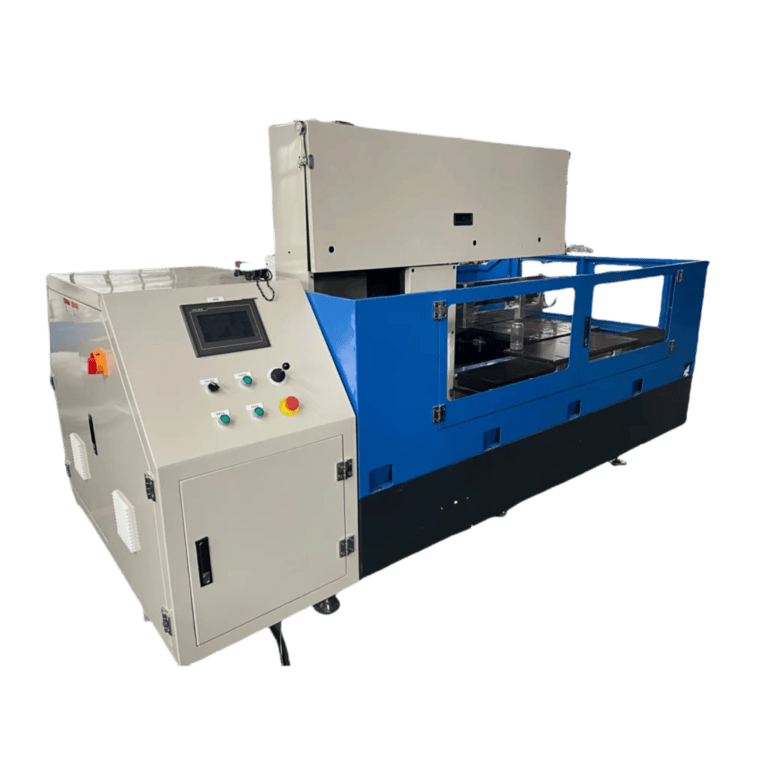
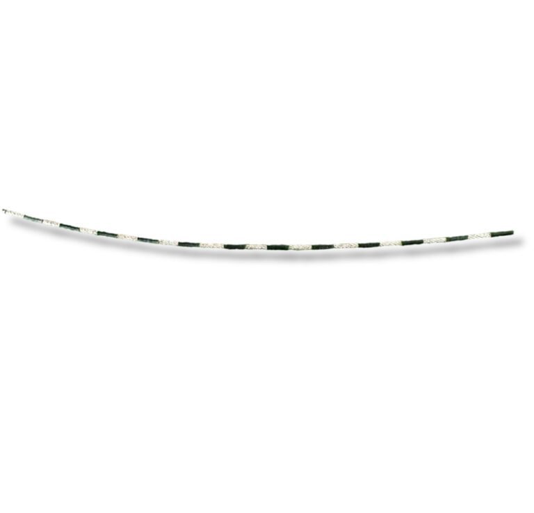
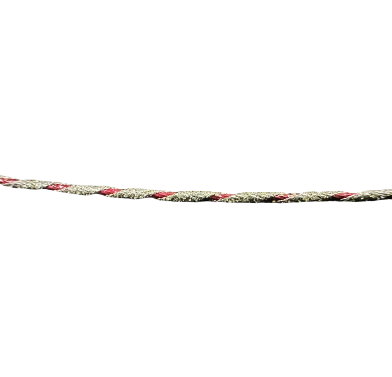
Diamond Wire Cutting Technology
One of the most advanced solutions for semiconductor wafer cutting is diamond wire cutting technology.
Diamond wire cutting systems use a wire embedded with diamond abrasives to grind through semiconductor materials. The cutting action is distributed along the moving wire, reducing mechanical stress on the wafer.
Typical operating parameters include:
- Wire speed up to 80 m/s
- Wire tension between 150–250 N
- Kerf width approximately 0.4 mm
These parameters allow precise material removal while maintaining high cutting efficiency.
Engineering Principles of Diamond Wire Cutting
Diamond wire cutting operates based on abrasive machining principles.
Distributed Cutting Force
Unlike blade-based cutting systems, diamond wire distributes cutting forces along a long section of moving wire. This significantly reduces localized stress.
Controlled Material Removal
The diamond particles embedded in the wire gradually grind away material, reducing the likelihood of crack propagation.
Thermal Stability
High wire speeds improve heat dissipation and prevent excessive thermal damage during the semiconductor wafer cutting process.
These engineering advantages make diamond wire cutting particularly suitable for brittle semiconductor materials.
Advantages of Endless Diamond Wire Cutting Machines
Endless diamond wire cutting machines provide several advantages in semiconductor manufacturing.
Low Kerf Loss
With a kerf width of approximately 0.4 mm, material waste during semiconductor wafer cutting can be significantly reduced.
Smooth Surface Quality
The grinding action of the diamond abrasives produces smoother wafer surfaces compared with traditional cutting methods.
High Precision
Stable wire tension and high wire speeds allow precise control of wafer thickness and flatness.
Suitable for Hard Materials
Diamond abrasives can effectively cut extremely hard materials such as silicon carbide and sapphire.
These advantages make endless diamond wire cutting machines an attractive solution for semiconductor manufacturers seeking higher efficiency and better wafer quality.
Industrial Applications of Semiconductor Wafer Cutting

Precision semiconductor wafer cutting equipment is used across a wide range of semiconductor industries.
Silicon Wafer Production
Silicon wafers are the foundation of modern integrated circuits. High-precision cutting ensures thickness uniformity and minimal surface damage.
Silicon Carbide Power Devices
Silicon carbide wafers are widely used in high-voltage power electronics. Their extreme hardness requires advanced cutting technologies.
Sapphire Substrates
Sapphire wafers are commonly used in LED production and optical devices. Precise cutting ensures optical quality and dimensional stability.
Compound Semiconductors
Materials such as gallium arsenide and gallium nitride are used in RF devices and optoelectronics, requiring careful cutting to prevent structural defects.
Future Trends in Wafer Cutting Technology
As semiconductor technology evolves, the requirements for semiconductor wafer cutting continue to increase.
Harder Semiconductor Materials
Wide-bandgap materials are becoming more common in power electronics and high-frequency devices.
Larger Wafer Sizes
Increasing wafer diameter improves manufacturing efficiency but requires more stable cutting systems.
Higher Precision Requirements
Advanced semiconductor nodes demand tighter control of wafer thickness, surface integrity, and dimensional accuracy.
Equipment manufacturers are therefore developing more advanced cutting technologies to meet these demands.
Conclusion
Precision wafer slicing is a fundamental step in semiconductor manufacturing. From traditional mechanical saws to modern diamond wire cutting machines, semiconductor wafer cutting technology continues to evolve to meet the challenges of processing hard and brittle materials.
Advanced cutting equipment improves wafer quality, reduces material waste, and increases manufacturing efficiency. By adopting modern solutions such as endless diamond wire cutting systems, semiconductor manufacturers can achieve more reliable and cost-effective wafer production.