The semiconductor industry relies on highly specialized manufacturing systems to produce wafers used in integrated circuits, power electronics, and optoelectronic devices. Each production stage requires carefully engineered machinery capable of operating with extremely tight tolerances.
The term wafer fabrication equipment refers to the machines used for crystal growth, wafer slicing, surface preparation, and inspection during wafer production. These systems must provide high dimensional accuracy while minimizing mechanical damage to brittle semiconductor materials.晶圆制造设备是指在晶圆生产过程中用于晶体生长、晶圆切片、表面处理和检测的机器。这些系统必须提供高尺寸精度,同时尽量减少脆性半导体材料的机械损伤。
For semiconductor manufacturers, selecting the appropriate equipment is essential for improving yield, reducing production costs, and maintaining consistent wafer quality.
This article provides an overview of the key machines used in wafer fabrication and explains how advanced cutting technologies improve wafer processing efficiency.
Overview of the Wafer Fabrication Process晶圆制造工艺概述
Wafer fabrication begins with the production of single-crystal semiconductor materials and continues through several precision machining and finishing stages.
Typical process steps include:典型的处理步骤包括:
- Crystal growth
- Ingot shaping and orientation
- Wafer slicing
- Edge grinding
- Lapping and polishing
- Cleaning and inspection
Each stage requires specialized wafer fabrication equipment designed to maintain tight process control and reduce surface defects.
Crystal Growth Systems
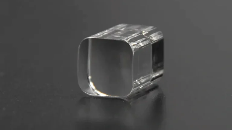
The first stage of wafer production is the growth of a single-crystal ingot.
Czochralski Crystal Pullers

The Czochralski method is widely used to produce silicon crystals. A seed crystal is dipped into molten silicon and slowly pulled upward while rotating.
Careful control of temperature and pulling speed allows the formation of large, high-quality silicon crystals.
Silicon Carbide Growth Systems
For wide-bandgap materials such as silicon carbide, physical vapor transport reactors are commonly used.
These systems operate at extremely high temperatures and require precise control of thermal gradients to ensure crystal quality.
The ingots produced in this stage are later processed using downstream wafer fabrication equipment
Ingot Processing Equipment
After crystal growth, the ingot must undergo mechanical preparation before wafer slicing.
Cylindrical Grinding Machines
Grinding machines remove surface irregularities and produce ingots with precise diameters.
Orientation and Notching Systems
These systems determine the crystal orientation and create flats or notches used for alignment during semiconductor manufacturing.
Wafer Slicing Equipment 晶圆切片设备
Wafer slicing converts large semiconductor ingots into thin wafers.
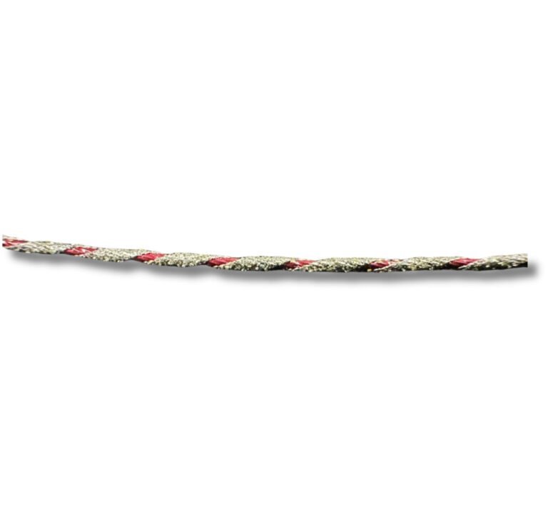
Traditional slicing machines include:
- Inner diameter saws 内径锯
- Multi-wire slurry saws
- Fixed abrasive wire saws
However, harder materials such as silicon carbide and sapphire require more advanced wafer fabrication equipment to achieve precise cutting while minimizing kerf loss.。
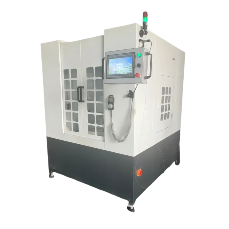
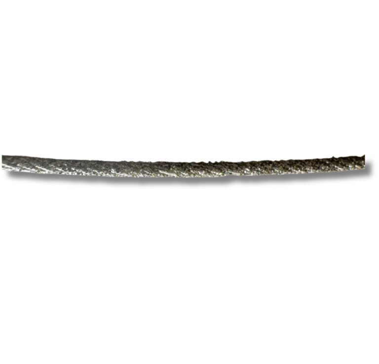
Endless Diamond Wire Cutting Technology
An advanced slicing solution is the endless diamond wire cutting machine.
Typical parameters include:
- Wire speed up to 80 m/s
- Wire tension 150–250 N 150–250 N
- Kerf width about 0.4 mm
The diamond abrasives remove material through grinding, which reduces mechanical stress during cutting.
다이아몬드 와이어 커팅의 장점
Integrating diamond wire systems into wafer fabrication equipment offers several benefits:
- Reduced kerf loss
- Improved surface integrity
- High dimensional accuracy
- Capability for hard and brittle materials
These advantages help manufacturers improve wafer yield and reduce processing costs.
Surface Finishing Equipment
After slicing, wafers must undergo surface finishing processes to remove mechanical damage.
Lapping Machines
Lapping improves wafer flatness by removing surface irregularities using abrasive slurry.
Chemical Mechanical Polishing (CMP)
CMP systems combine chemical reactions and mechanical polishing to produce extremely smooth wafer surfaces required for photolithography.
Cleaning Systems
Cleaning equipment removes particles, residues, and contaminants from wafer surfaces before semiconductor device fabrication begins.
Maintaining ultra-clean surfaces is essential for achieving high manufacturing yield.
Inspection and Metrology Equipment
Quality control plays an essential role in wafer production.
Inspection systems measure key parameters such as:
- Wafer thickness
- Surface roughness
- Flatness
- Edge defects
Laser-based and optical metrology tools help detect microscopic defects that could affect semiconductor device performance.
These inspection tools are important components of modern wafer fabrication equipment infrastructure.
Future Trends in Wafer Fabrication Equipment
The semiconductor industry continues to evolve rapidly, driving the development of new equipment technologies.
Larger Wafer Diameters
Increasing wafer size improves chip production efficiency but requires more advanced slicing and polishing equipment.
Harder Semiconductor Materials
Wide-bandgap materials such as silicon carbide and gallium nitride require machining technologies capable of processing extremely hard crystals.
Higher Precision Requirements
As semiconductor devices continue to shrink, wafer surface quality and dimensional accuracy become increasingly critical.随着半导体器件的不断缩小,晶圆表面质量和尺寸精度变得越来越重要。
Manufacturers must therefore adopt more advanced machining and inspection technologies.
자주 묻는 질문 常见问题解答
What equipment is used in wafer fabrication?
Wafer fabrication requires multiple types of equipment, including crystal growth systems, wafer slicing machines, grinding equipment, polishing systems, cleaning tools, and inspection instruments.
Why is wafer slicing equipment important?
Wafer slicing determines wafer thickness uniformity, material utilization, and surface quality, all of which directly affect semiconductor device yield.
What materials are commonly processed in wafer fabrication?
Common materials include silicon, silicon carbide, gallium nitride, gallium arsenide, and sapphire.
결론
Producing high-quality semiconductor wafers requires a wide range of advanced manufacturing systems. From crystal growth reactors to precision slicing and polishing machines, each stage of wafer production depends on specialized technology.
Modern wafer fabrication equipment plays a crucial role in improving wafer quality, reducing material loss, and increasing production efficiency.
By adopting advanced cutting technologies such as endless diamond wire systems, semiconductor manufacturers can achieve more efficient and stable wafer production.通过采用先进的切割技术,如无尽的金刚石线系统,半导体制造商可以实现更高效和稳定的晶圆生产。