
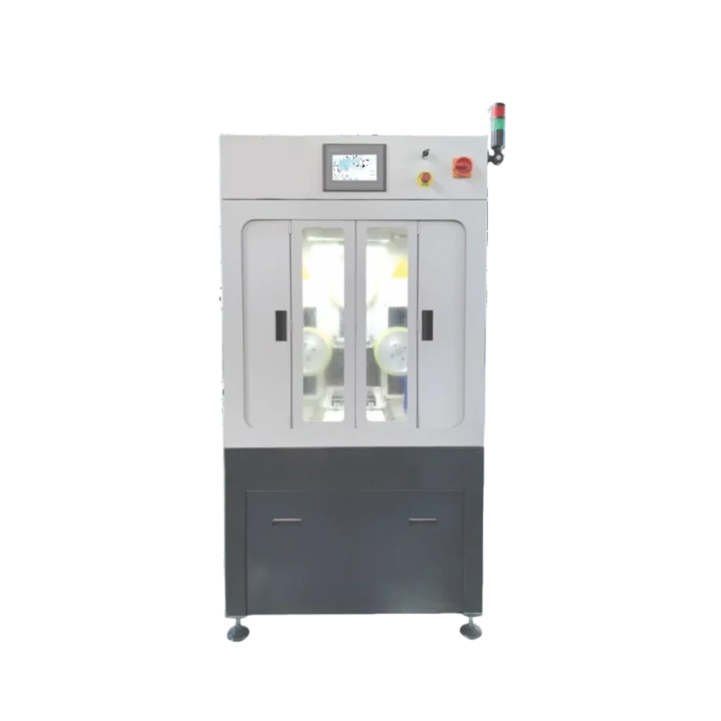
先端セラミック&材料用精密半導体切断装置
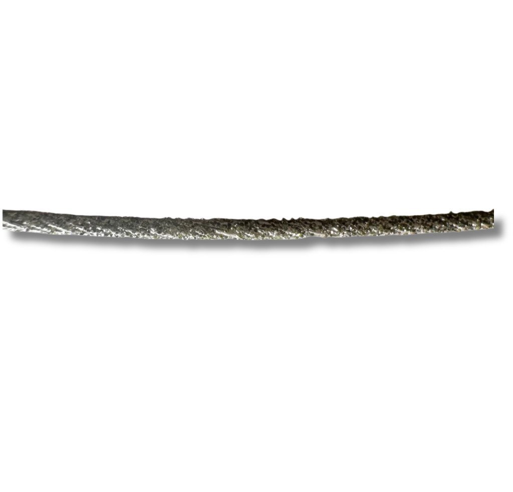
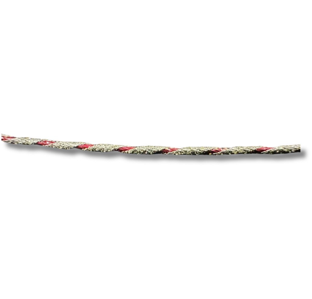
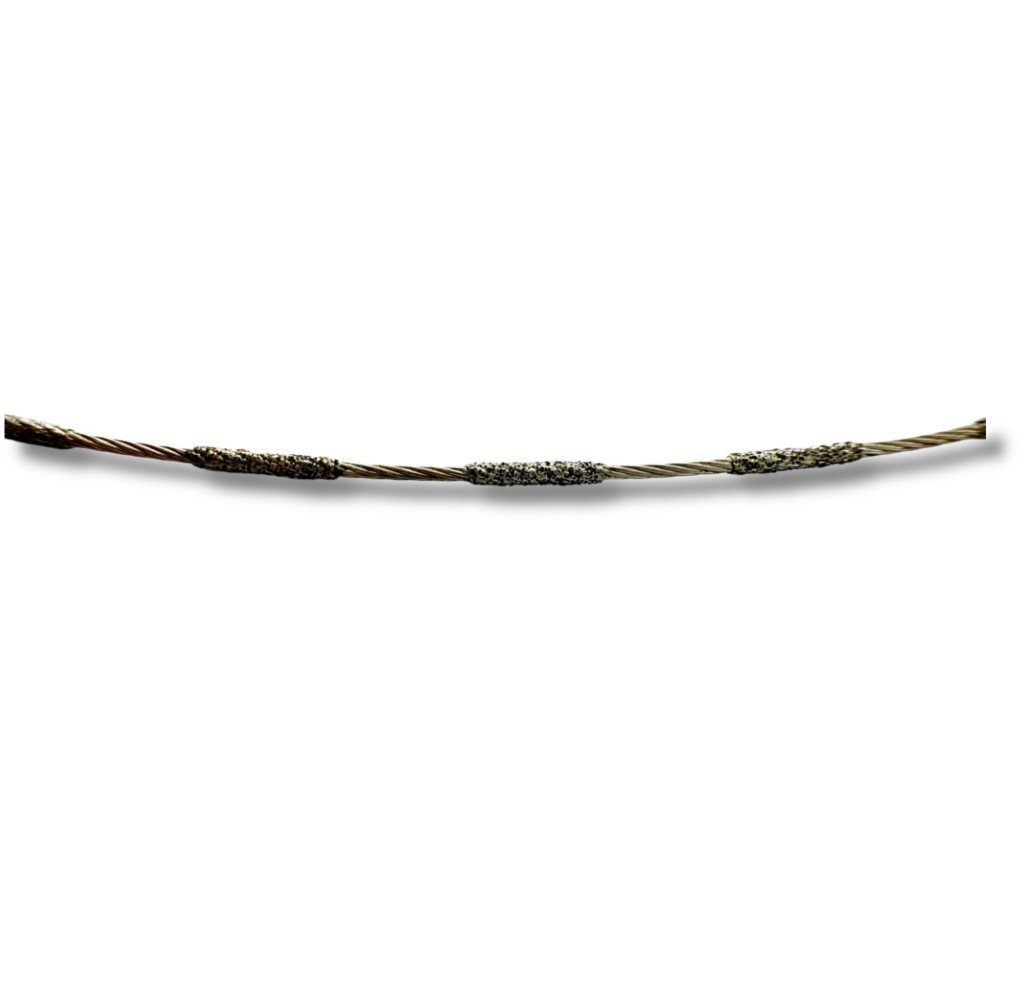
シリコン、SiC、サファイア、セラミックウエハーに最適化されたダイヤモンドワイヤー技術による半導体切断装置。
N .オフィス
カナダ、MB州ウィニペグ
お電話でのお問い合わせ
(1)408-571-8651
午前7時30分~午後7時30分
7日
事業内容
硬脆材料用先進半導体切断装置
当社は、半導体および先端エレクトロニクス産業で使用される超硬質、脆性、高価値の材料に合わせた精密ダイヤモンドワイヤー切断機を特徴とする半導体切断装置の設計と製造を専門としています。当社のソリューションは、ウェーハスライス、ロッド分割、輪郭切断、インナーホール切断をカバーし、クリーンで低カーフの結果を保証します。プログラマブルオートメーションと完全なプロセス制御を備えた当社の半導体切断装置は、お客様の生産ニーズに対して高い精度と効率を保証します。
無料サンプルカット
私達は工作物およびデッサンを送れば試供品の切口を提供します
マシンデザイン
お客様の切断ニーズに合わせた機械の設計
消耗品
スムーズなマシン操作に必要な消耗品をすべて提供
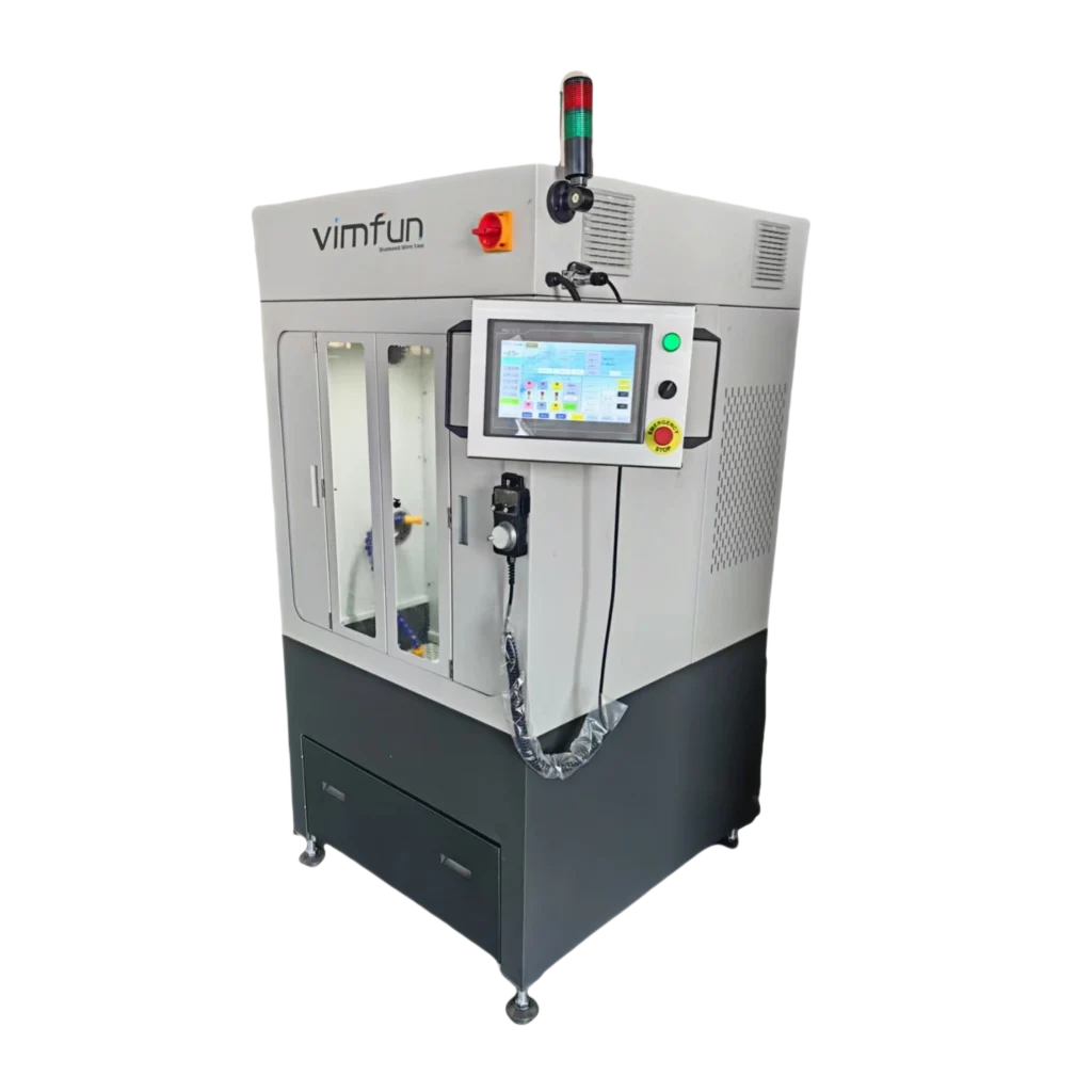
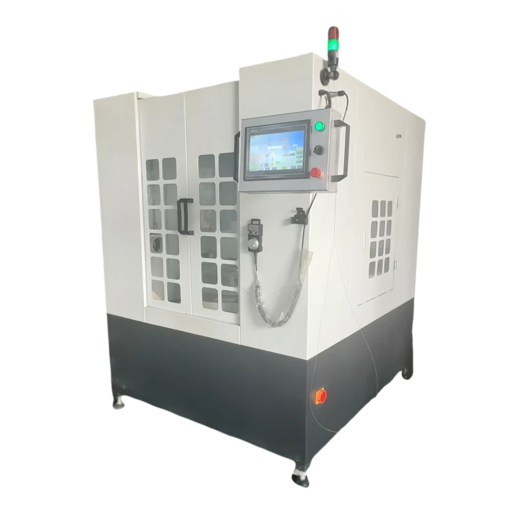
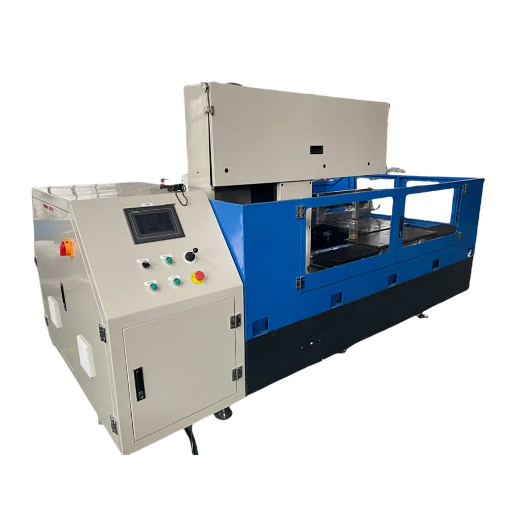
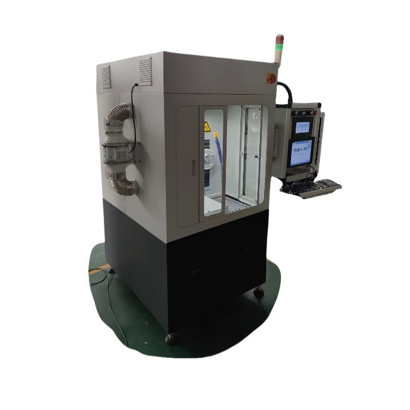
カッティング・マシー
先進の半導体切断装置
薄いウェハーのスライスから複雑な輪郭の切断まで、当社の半導体切断装置は業界の幅広い作業に対応しています。アルミナ、シリコンカーバイド、サファイア、圧電セラミックのいずれを扱う場合でも、高精度の結果と効率的な操作を実現するために設計された、信頼性が高くカスタマイズ可能なソリューションを提供します。
カットする素材
精密級材料ソリューション用半導体切断装置
当社の半導体切断装置は、半導体材料メーカー、セラミック加工メーカー、フォトニクス企業から世界中で信頼を得ています。代表的なアプリケーションには、サファイアロッドのスライス、炭化ケイ素インゴットの分割、アルミナ基板の輪郭切断、超薄型圧電ウェハーの製造などがあり、クリーンなエッジ、最小限のチッピング、安定したスループットを実現します。
会社概要
当社の切断機が優れている理由
硬くて脆い材料の切断において長年の経験を持つ当社は、単なる機械ではなく、完全な切断ソリューションを提供します。当社の装置は、超低カーフロス、プログラマブルモーション制御、クリーンなスライス面、柔軟な構成オプションを特徴としています。グローバルなサポートと実際の成功に支えられ、より賢く、より速く、よりクリーンな切断をお手伝いします。
🔹 チップフリー・エッジ品質
超滑らかな表面仕上げ
カーフ・ロスの最小化
🔹 低切削応力
薄い素材から硬い素材まで 🔹 対応
クリーンルーム対応 🔹 動作
ニュース&インサイト
専門家による先取り
光学材料加工、切断技術、アプリケーション固有の課題に関する詳細な記事をご覧ください。